We’re living through a moment of inflexion, where classical electronic design begins to blur with the demands of quantum computing, photonics, and ultra-high-frequency systems. Amid this transformation, one material has quietly stepped into the spotlight: glass.
We’re talking about Glass PCBs—transparent, ultra-precise, and incredibly stable circuit substrates that are becoming indispensable in the design of tomorrow’s quantum and photonic devices.
So, why is glass making waves in an industry traditionally dominated by flexible polymers? The answer lies in three words: precision, purity, and potential.
What Exactly Is a Glass PCB?
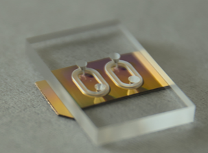
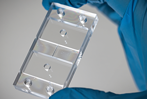
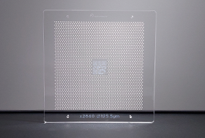
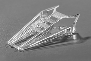
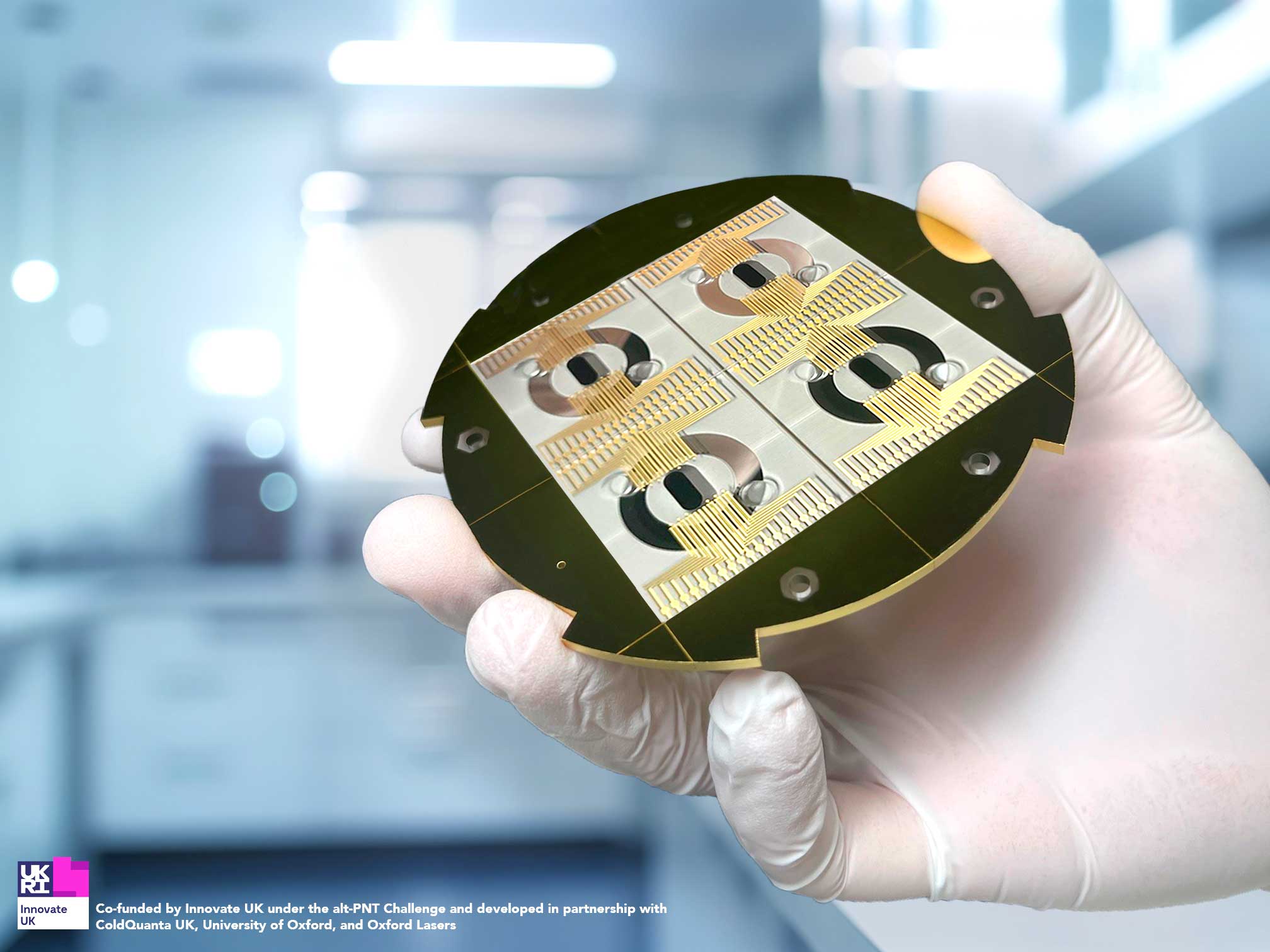
A Glass PCB (Printed Circuit Board) is a circuit board fabricated using glass or glass-ceramic substrates instead of standard composite materials like FR4. This isn’t just a stylistic pivot, it's a functional one.
Glass offers a unique set of properties:
For those designing quantum processors, photonic chips, or RF modules that demand impeccable signal fidelity, this is more than a materials upgrade; it’s a paradigm shift.
Why CTOs in Quantum and Advanced Electronics Should Care?
If you're leading R&D or architecture decisions in quantum computing, photonics, or high-frequency electronics, here’s why Glass PCBs should be on your radar:
1.Temperature Stability Under Fire
In environments where thermal drift can ruin calibration—or worse, decohere your quantum state—glass substrates offer ultra-low thermal expansion. They don’t move, bend, or flex under temperature changes, preserving interconnect accuracy and optical alignment in cryogenic setups.
2.Perfect for High Frequencies
Glass boasts a low dielectric constant and minimal loss tangent, making it ideal for GHz to THz signal paths. For quantum RF control systems, readout lines, or superconducting qubits, the dielectric performance of glass minimizes signal degradation.
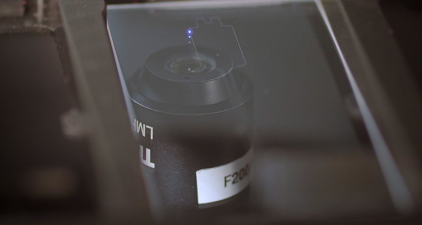
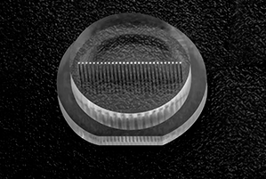
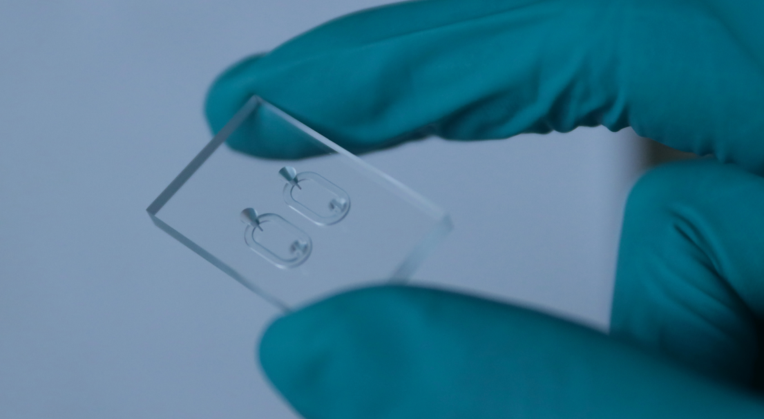
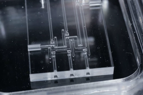
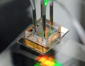
3.Ready for Photonics
Here’s where things get exciting. Because it’s transparent, glass PCB technology allows for the co-integration of optical waveguides, mirrors, and electrical traces on the same substrate. That’s a game-changer for photonic integrated circuits (PICs) and quantum optical processors.
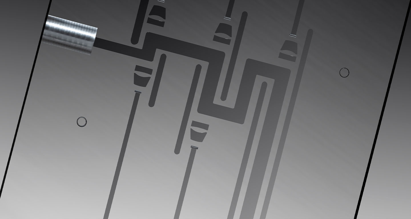
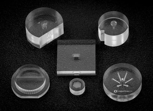
4.Precision Fabrication
Using tools like femtosecond lasers, ultrafast micromachining, and direct-write lithography, manufacturers can produce vias, traces, and alignment marks with extreme fidelity. That’s vital when tolerances in your quantum photonic device are measured in nanometers.
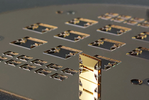
Where Is This Technology Being Used?
Today, Glass PCBs are making quiet but significant appearances in:
The Quantum-Ready Future Is Clear (Literally)
As quantum systems scale, and photonics moves from research labs into commercial products, materials like glass will no longer be fringe, they'll be fundamental.
Glass PCBs are not just substrates. They’re platforms for integration, precision, and reliability. For the CTO looking to future-proof their architecture—be it in quantum hardware, integrated photonics, or RF infrastructure—glass is more than transparent. It’s transformative.
If you're pushing the limits of what's technically possible, you need tools—and materials—that can keep up. Glass PCBs offer the rare combination of:
In short: they’re not just the next big thing. They’re already here, quietly enabling the future.
What we can do:
Schedule a free consultation with our expert today.