What does glass microdevice contract development actually involve?
Contract development is not prototyping. It is the structured engineering work that makes a device manufacturable, repeatable, and certifiable, before committing to production tooling or volume investment.
Through our proven vertical integration strategy, we have spent the past decade becoming specialists across a vast range of manufacturing processes. At FEMTOPRINT, we seamlessly combine research, product development, and industrialized manufacturing to create high-impact, meaningful products.
We serve as a strategic one-stop shop for development, manufacturing, testing, and assembly. By integrating Design for Manufacturing (DfM) and Design for Assembly (DfA) from the earliest stages, we eliminate unnecessary margin-on-margin costs and guarantee maximum flexibility, delivering both agile prototyping and cost-efficient microfabrication.
Our customers' competitive edge starts at FEMTOPRINT. Our deep expertise in designing for manufacturing, testing, and assembly provides a critical contribution to the overall success of every project. Whether it involves wafer-level manufacturing, ultrafast laser processing, 3D glass structuring, or complex microsystem integration, we ensure your product is optimized for the market.
What feature sizes and geometries are achievable?
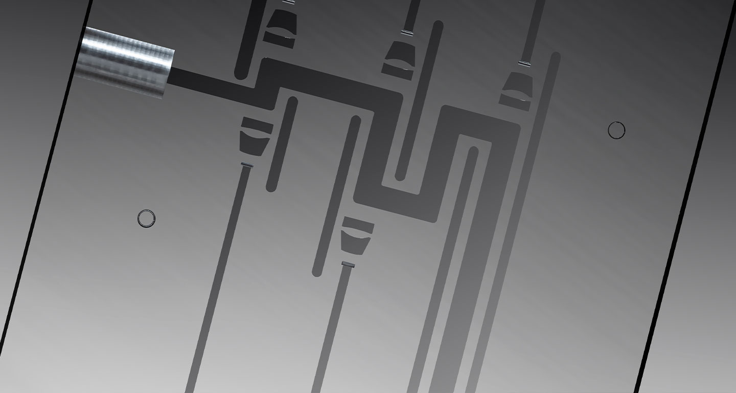
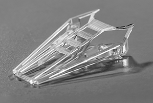
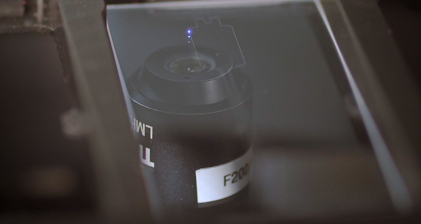
FEMTOPRINT's femtosecond laser platform modifies the glass bulk volumetrically, not just at the surface. This enables true 3D geometries: buried channels, internal cavities, undercuts, stacked microfluidic networks, and through-glass vias, all in a single monolithic piece without bonding or assembly.
Typical specifications achievable in contract development:
These are not theoretical limits, they are process-qualified parameters available from the first prototype run.
Is this service suitable for regulated markets?
Yes. FEMTOPRINT SA is certified ISO 13485:2016 for medical device manufacturing and ISO 9001:2015 for general industrial quality management. Contract development projects targeting regulated applications, active implantable devices, in-vitro diagnostic components, drug delivery systems, are managed under our certified QMS from the first design review through pilot production.
We routinely sign NDAs before the first technical conversation. All project data, CAD files, process recipes, and characterization results are handled under strict confidentiality protocols and never shared outside the project team.
How do you start a contract development project with FEMTOPRINT?
You do not need complete CAD files to begin. A clear problem statement, a sketch, and a set of target specifications are sufficient for a first conversation.
The process: submit a contact request or call our engineering team directly. Within one week of a first technical exchange, you receive a written feasibility assessment and a project proposal covering scope, timeline, and cost structure. The initial consultation is complimentary and covered by NDA from the first exchange.
The fastest projects begin with a customer who has already answered three questions internally: what does the device need to do, what are the critical dimensions, and what is the target market or regulatory context. Everything else we develop together.
What is Selective Laser Etching (SLE)?
Selective Laser Etching is a two-step glass microfabrication process. A femtosecond laser writes a defined 3D path inside the bulk glass, locally modifying the material. A selective wet etch then removes the laser-modified regions far faster than the untouched glass, revealing true three-dimensional structures with no mask and no mould.
How are 3D microchannels made in glass?
A femtosecond laser is focused inside the glass and traces the channel path in three dimensions. Because it modifies only the focal volume, the path can curve and branch through the bulk. A selective etch then opens the modified track, producing buried microchannels that conventional masked etching cannot reach.
What is the difference between femtosecond laser machining and wet etching for glass?
Conventional glass micromachining masks the surface and etches downward, which limits geometries to roughly 2.5D. Selective Laser Etching uses a femtosecond laser to define the geometry directly inside the bulk before a selective etch, so genuine 3D free-form features, buried channels and angled structures become possible in a single monolithic part.
What is the smallest feature size achievable in glass microfabrication?
Achievable resolution depends on the geometry, glass type and functional tolerance, so it is defined per project during the feasibility review. As documented references, FEMTOPRINT reaches positioning and diameter tolerances down to about ±0.5 µm on glass ferrules, optical shape accuracy down to 0.2 µm, and surface roughness down to roughly 5 nm.
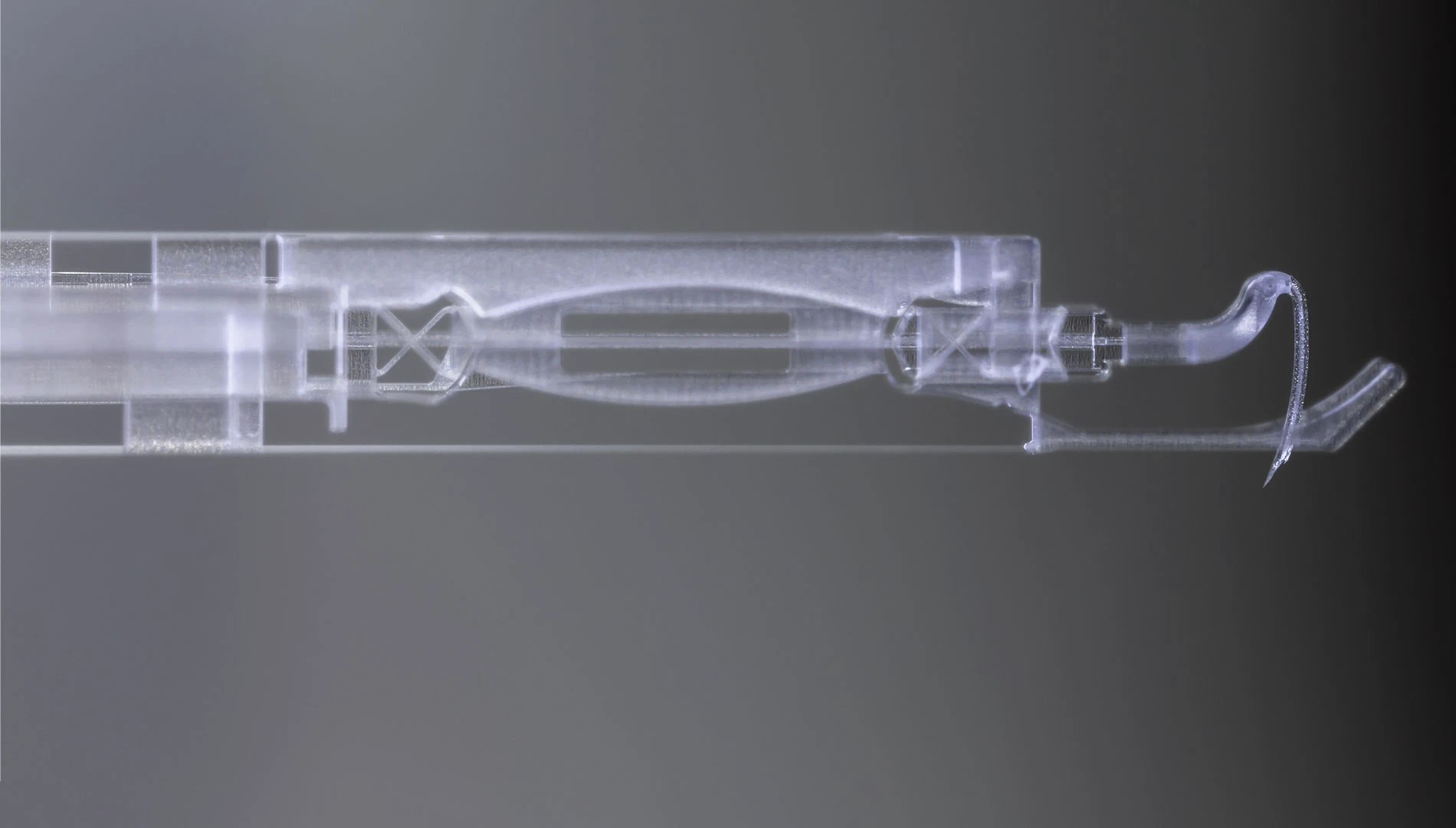
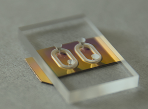
Can you fabricate buried channels inside fused silica?
Yes. Buried channels are a core strength of Selective Laser Etching. The femtosecond laser defines the channel inside the bulk fused silica and a selective etch opens it, leaving the surrounding glass intact. This enables sealed, monolithic microfluidic and photonic structures without bonding two separate plates.
How is glass microfabrication different from silicon MEMS?
Silicon MEMS rely on planar lithography, which favours layered 2.5D structures. Glass adds optical transparency, electrical insulation, chemical inertness, biocompatibility and low autofluorescence. Combined with femtosecond selective laser etching (SLE), glass allows true 3D free-form geometries, making it well suited to photonics, microfluidics, quantum and medtech devices.
Start with a feasibility review
Send us your drawing or functional requirement. We will tell you what is manufacturable, where the design can be relaxed, and how it scales, before you commit to tooling.
 Cutting-edge engineering competencies – Where technology meets brilliant minds
Unique technology platform – Enabling free-form, high-precision glass microdevices
Efficient Project Management – A “building blocks” approach configured in such way that there is a perfect match with the Customer needs
Design for Manufacturing – We ensure that proper tools are used to allow reliable, manufacturable devices up to volumes manufacturing
Cutting-edge engineering competencies – Where technology meets brilliant minds
Unique technology platform – Enabling free-form, high-precision glass microdevices
Efficient Project Management – A “building blocks” approach configured in such way that there is a perfect match with the Customer needs
Design for Manufacturing – We ensure that proper tools are used to allow reliable, manufacturable devices up to volumes manufacturing