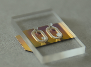
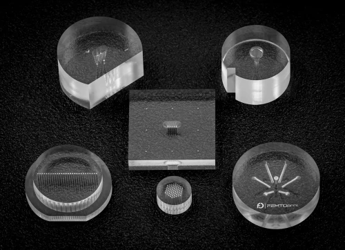
Glass waveguides and related beam routing, splitting, and coupling devices
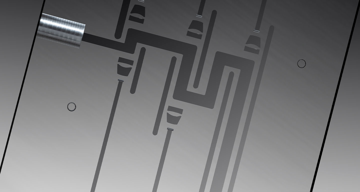
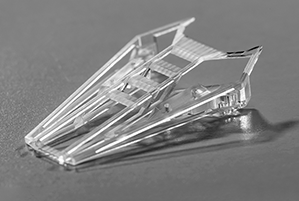
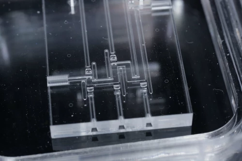
As photonic systems become more complex, traditional fabrication techniques often fall short in flexibility and integration. FEMTOPRINT’s platform enables the direct writing of 3D glass waveguides for beam routing, splitting, and coupling, offering true volumetric freedom.
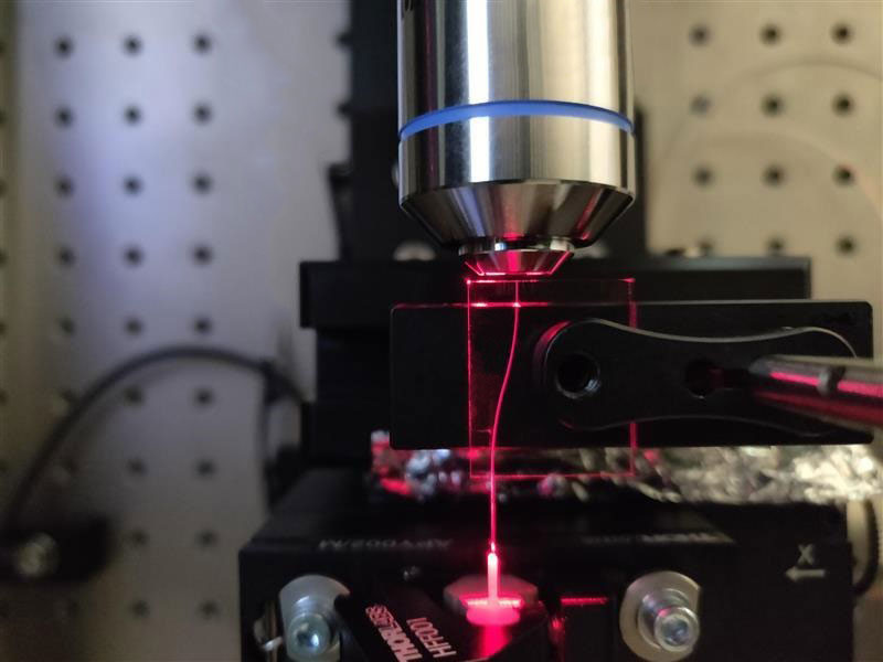
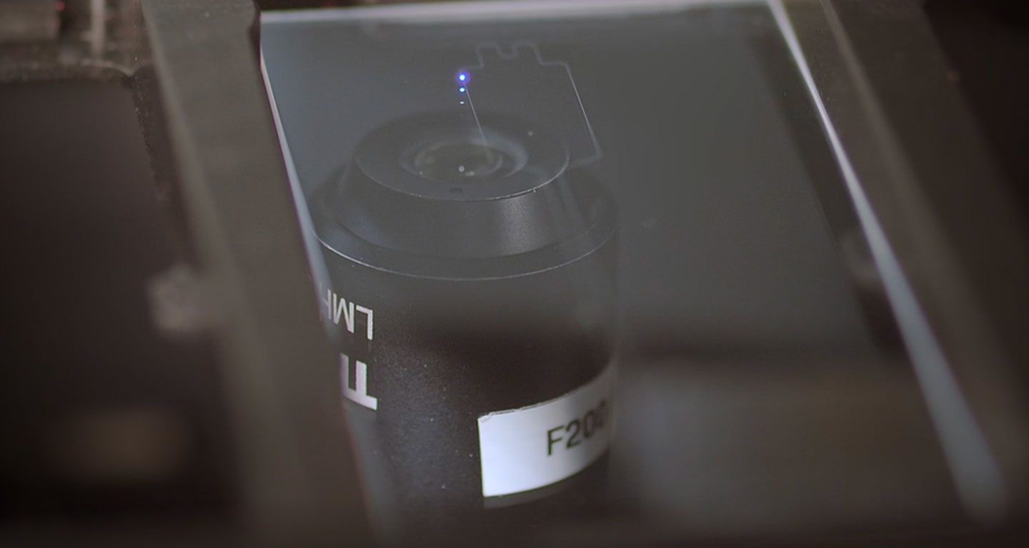
Using ultrafast laser pulses, we can write refractive index-modulated patterns directly within fused silica or borosilicate glass wafers—ideal for light coupling, beam steering, or multi-channel routing.
Our approach allows:
%20(1).png)
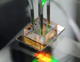
Whether you are building a PIC, a quantum device, or a fiber array interface, our laser-written waveguides provide the precision and flexibility that other solutions cannot match.
FEMTOPRINT’s advanced laser micro-machining technology enables localized refractive index modification in glass, achieving changes in the range of 10⁻² to 10⁻³.
This capability is essential for the fabrication of embedded 3D optical waveguides within the bulk of transparent substrates, unlocking new opportunities in the design and integration of photonic integrated circuits (PICs) and optical interconnects.
With this laser-based process, it is possible to precisely manufacture both single-mode and multimode optical waveguides at key telecommunications wavelengths, specifically 1310 nm and 1550 nm. Additional optical components—such as tapered waveguides, mode converters, fan-in/fan-out structures, and more—can also be seamlessly integrated, supporting the development of compact, high-performance photonic devices for next-generation applications.
Discover more about biophotonics here
 Wavelenght range 650-1550nm.
Min mode field diameter 6-8um at 1000nm-1550nm, respectively
Propagation losses <0.2dB/cm.
Min bending radious 20-25mm at 1000nm-1550nm.
Materials: fused silica, borofloat 33, Eagle XG.
Wavelenght range 650-1550nm.
Min mode field diameter 6-8um at 1000nm-1550nm, respectively
Propagation losses <0.2dB/cm.
Min bending radious 20-25mm at 1000nm-1550nm.
Materials: fused silica, borofloat 33, Eagle XG.