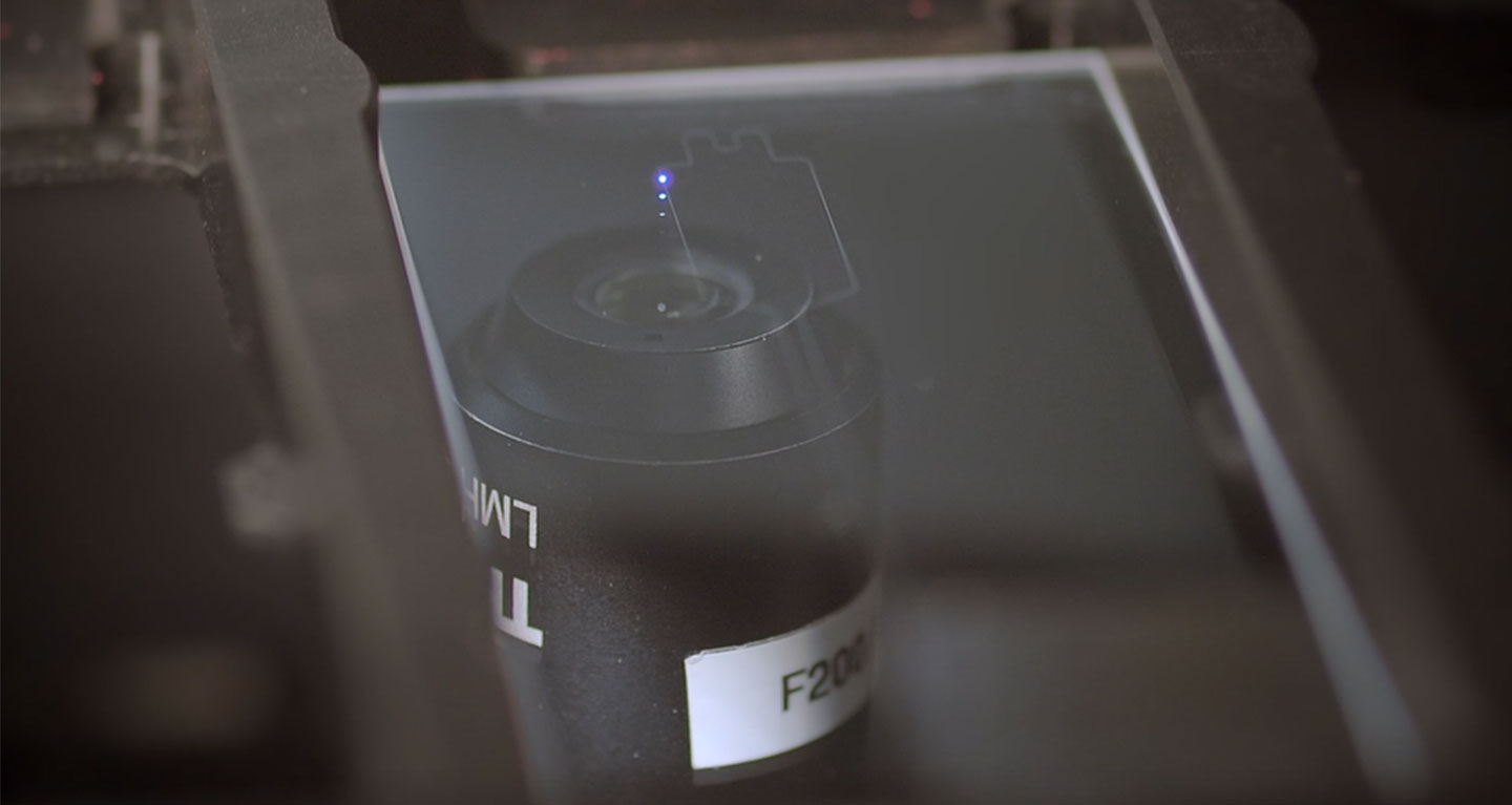
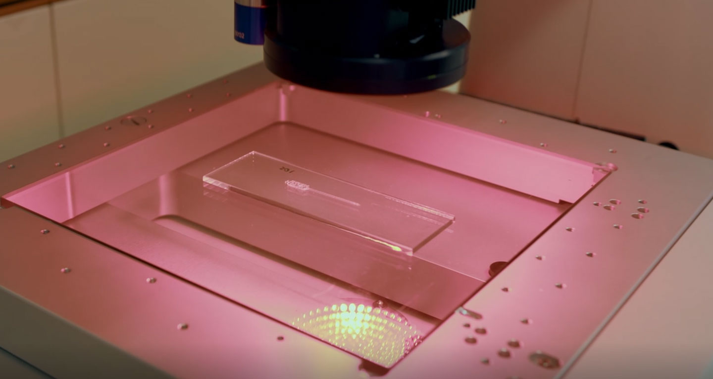
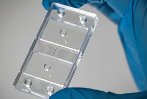
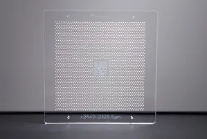
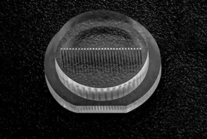
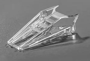
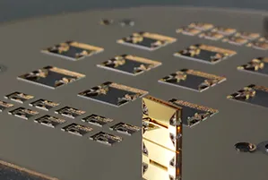
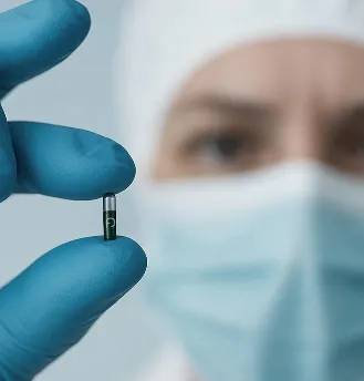
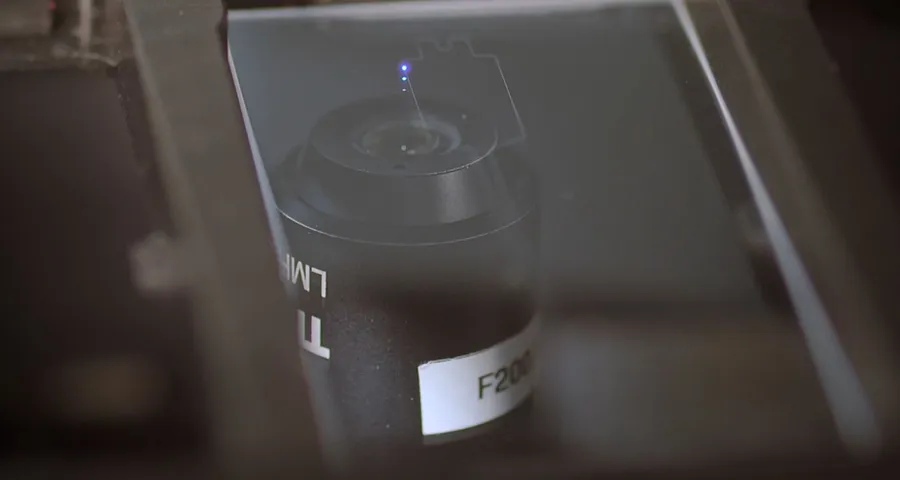
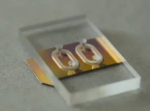
Maskless glass microfabrication uses a tightly focused femtosecond laser to write three-dimensional structures directly into the volume of the glass, no photomasks, no lithography steps, no layer bonding. FEMTOPRINT applies this process to manufacture monolithic glass microdevices with ±1 µm accuracy in XY (±2 µm in Z), features below 5 µm, and aspect ratios up to 1:500, from single prototypes to wafer-scale production on substrates up to 300 mm.
What does maskless laser processing change?
Conventional glass microstructuring depends on photomasks: every design change means a new mask, new alignment steps, and weeks of added lead time. In a maskless process, the design lives in the toolpath. The femtosecond laser modifies the glass only at its focal point, so a revised geometry can move from CAD file to physical part without any new tooling.
For R&D teams, this compresses design iteration from weeks to days. For production, it means the same process qualified on your prototype scales to volume without re-engineering, the geometry that worked on one part is written identically on hundreds of thousands.
Monolithic 3D parts: no bonding, no assembly
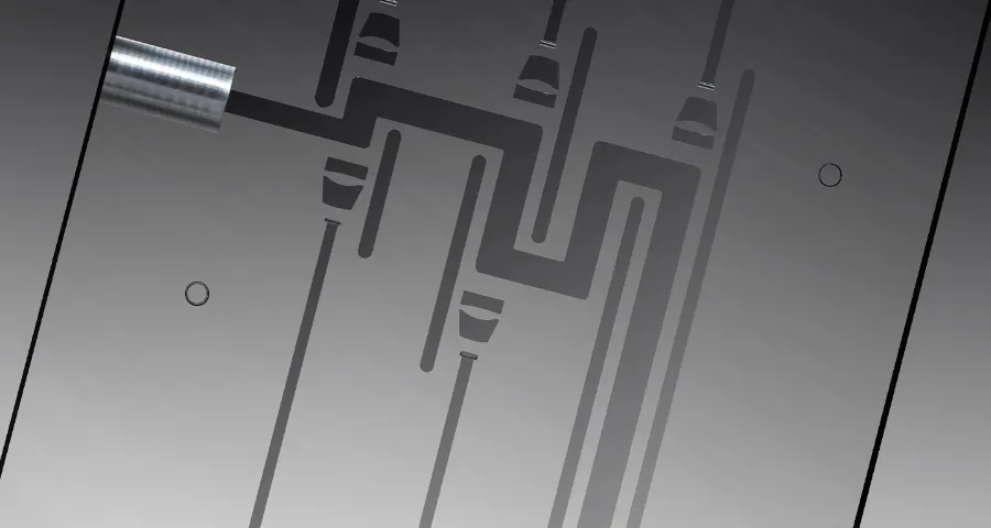
Because the laser writes inside the bulk material, channels, cavities, optical elements and mechanical features are formed within a single piece of glass. There are no bonded layers, no adhesives in the fluidic path, and no alignment tolerances stacking up between components. The result is a monolithic part with free-form 3D geometries undercuts, buried channels, curved internal surfaces, that multi-layer fabrication approaches cannot reproduce.
From first concept to certified production
FEMTOPRINT operates as a full-service CDMO: feasibility analysis, design-for-manufacturing support, prototyping, process qualification and wafer-scale series production under one roof in Switzerland. Manufacturing runs under ISO 13485:2016 and ISO 9001:2015, with the documentation and traceability that medtech, photonics and aerospace programs require. More than 250 OEM partners across 35+ countries build on this process today.
What drives innovation in precision glass microdevice manufacturing?
FEMTOPRINT is synonymous with innovation, our skilled process engineers are poised to impress.
In the realm of precision and miniaturization, innovation isn't a choice; it's a necessity. Our team lives and breathes innovation. We are constantly pushing boundaries and redefining what's possible in microdevice manufacturing.
How do FEMTOPRINT engineers turn R&D concepts into reliable manufacturing processes?
Our engineers turns customer ideas and R&D concepts into reliable manufacturing processes. With a multitude of expertise, they're always finding new ways to cut down costs, enhance processes and the equipment we operate to create your glass devices.
How does FEMTOPRINT ensure process reliability and customer support as standard?
Through meticulous documentation, risk analysis, and rigorous testing, we ensure seamless operations. Above all, we give our customers, as standard, smarter solutions and an unparalleled degree of support. Highly competitive products are a good start, but at FEMTOPRINT we do a lot more.
Join us today in embracing innovation
How accurate is femtosecond laser glass microfabrication?
FEMTOPRINT's process achieves ±1 µm positional accuracy in XY and ±2 µm in Z, with minimum feature sizes below 5 µm and surface roughness below Sa 10 nm after post-treatment.
What makes the process maskless?
The femtosecond laser modifies glass only at its focal point, writing the geometry point by point from a digital toolpath. No photomasks or lithography steps are required, so design changes carry no tooling cost or delay.
Can the process scale to production volumes?
Yes. The same maskless process used for prototyping runs at wafer scale on substrates up to 300 mm, supporting series production of hundreds of thousands of units per year under ISO 13485:2016 and ISO 9001:2015.
Which materials can be structured?
The process is optimized for glass, primarily fused silica, chosen for its optical transparency, thermal stability and chemical inertness. Material selection for a specific application is defined during feasibility review.
 Maskless technology, ensuring fast turnaround cycles in prototyping
3D microfabrication in a monolithic fashion, avoiding costly alignment and assembly steps
3D shape accuracy ≈ 1µm
Maskless technology, ensuring fast turnaround cycles in prototyping
3D microfabrication in a monolithic fashion, avoiding costly alignment and assembly steps
3D shape accuracy ≈ 1µm