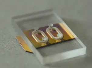
The recent massive implementation of Artificial Intelligence (AI) and the consequent need for the hyper-scalers to deploy new datacentres ensuring low energy consumption and latency with large bandwidth and high transmission speed is driving the development of innovative optical transceivers, including co-packaged optics (CPO) solutions and the integration of photonic integrated circuits (PICs) partly replacing electrical with optical data transmission.
This requires the implementation of new optical interconnects to enable ultralow-loss fibre-to-chip connectivity.
At the intersection of innovation and precision, FEMTOPRINT empowers engineers and system designers with cutting-edge solutions for glass micro-connectors monolithically integrating micro-optical devices with micro-mechanical and photonic components. The integration of multiple functionalities is indeed a key-aspect mostly driven by the need for parallelization, serialization, smaller footprint, enhancement of the optical performance, simplification of the assembly processes without loss of performance, immediate availability, at large volumes, and competitive prices.
Our focus lies in 3D glass microfabrication of advanced optical interconnects to enable extensive, cost-effective deployment while simultaneously expanding system functionalities.
Tackling Today’s Challenges in Integrated Photonics
With the introduction of PICs as key components for the new generation of optical transceivers, the industry faces growing demands for precision, scalability, and cost-effectiveness.
We serve clients who need precise microfabrication technologies to manufacture efficient ultralow-loss PIC-to-fibre optical interconnects based on the monolithic integration of micro-optical, micro-mechanical and photonics devices. Key challenges include:
Common Pain to Solve in the Photonics Market?
Our clients needs:
Our Value Proposition
Here, how we meet those needs:
The above unique selling points enable us to directly support demands for high-throughput production of glass micro-components for fiber-to-fiber and fiber-to-chip connectivity.
What We Deliver
What Sets Us Apart
Whether you are exploring fiber-to-chip or fiber-to-fiber optical connectivity, beam routing, beam shaping, optical coupling into quantum devices or biomedical/biophotonic systems FEMTOPRINT is your trusted partner in innovation.
Contact us to explore what we can create together.
As AI hyperscalers move data optically, the connector becomes the bottleneck. FEMTOPRINT builds the glass optical interconnects that co-packaged optics needs, monolithic fibre-to-chip routing at wafer scale.
| Parameter | Value |
|---|---|
| 3D waveguides written in the bulk of the glass | mode-field diameter 8–9 µm at 1550 nm |
| Propagation loss | 0.25 dB/cm |
| Coupling loss | 0.15 dB/facet |
| Crosstalk | below –30 dB at 20 µm pitch |
| Self-alignment of integrated elements | within ±1 µm |
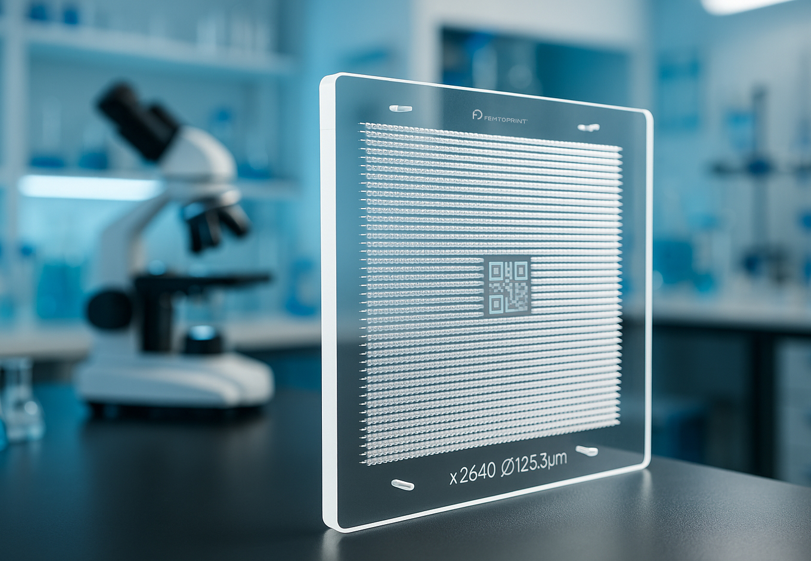
| Wafer-scale production | up to 200 × 200 mm |
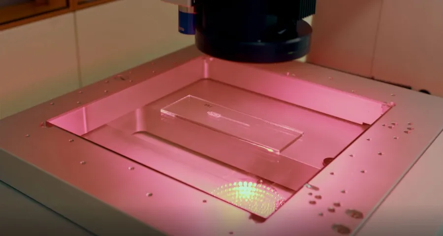
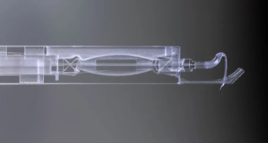
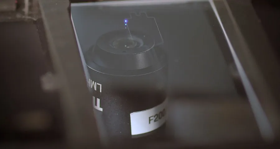
Monolithic glass components that route light between fibre and chip in co-packaged optics and PIC-based transceivers. Femtosecond-laser writing combines waveguides, micro-optics and alignment features in one glass body, replacing assembled multi-part interconnects.
Femtosecond-written 3D waveguides reach 0.25 dB/cm propagation loss and 0.15 dB/facet coupling loss, with a mode-field diameter of 8–9 µm at 1550 nm and crosstalk below –30 dB at 20 µm pitch.
Yes. Wafer-level production up to 200 × 200 mm scales from prototyping to high-volume manufacturing, which is what AI-datacenter optical interconnect deployment requires.
Monolithic glass self-aligns its integrated elements within ±1 µm, removing assembly steps, lowering packaging cost and improving optical performance versus multi-part interconnects.
Yes. Glass fibre ferrules with 1D/2D micro-hole arrays or V-grooves, plus 3D waveguides with couplers, splitters, spot-size converters and fan-in/fan-out structures, support both.
 In-glass photonic wire-bonding.
Monolithic integration of photonics functions.
Free-form fabrication in 3D, including design for manufacturing.
Combination of 3D bends, tapers & mode converters with low-loss glass waveguides.
Precise integration with hole arrays, V-grooves, and micro-optics.
Self-alignment of all elements within +/- 1 µm.
Thermal stability and optimized thermal properties for integrated photonics.