Most laser shops cut and drill glass in 2D. We build it in three dimensions.
FEMTOPRINT is a Swiss CDMO that turns complex glass microdevice concepts into certified, repeatable production, using femtosecond-laser Selective Laser Etching
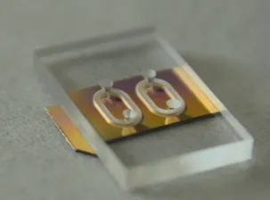
(SLE) to fabricate true 3D free-form geometries, buried microchannels and optical features inside a single monolithic substrate. Tolerances to ±1 µm (XY) / ±2 µm (Z),
features below 5 µm, and scaling from a single prototype to wafer-level batches up to 300 mm, all under one roof, ISO 13485 and ISO 9001 certified.
In the high-stakes fields of precision optics, quantum sensing, watchmaking and life sciences, innovation is the result of rigorous engineering.
At FEMTOPRINT, we don't just process glass; we engineer reliability. Our team of expert process engineers specializes in turning complex customer ideas into robust, cost-effective, and industrialized manufacturing workflows.
Our Engineering Edge:
Comprehensive Technical Support: We provide more than just a manufacturing service; we offer a strategic technical partnership. Our customers benefit from:
Our capabilities in glass microfabrication, ultrafast laser processing, and precision engineering ensure high-quality, scalable solutions for a wide range of industries including medtech, photonics, life sciences, quantum, and watchmaking.
With our vertical integration strategy, we became specialists in many advanced manufacturing processes over the past decade. At FEMTOPRINT we combine research, product development, process development and precision manufacturing to create meaningful, high-performance glass microdevices.
We serve as a one-stop shop for development, manufacturing, testing, and assembly. This enables us to eliminate margin over margin, reduce time-to-market, and guarantee highest flexibility—from rapid prototyping to wafer-level production.
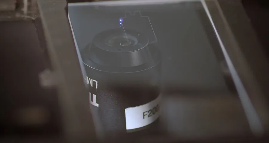
Standard laser cutting and HF/DRIE etching are essentially 2D or 2.5D processes. FEMTOPRINT uses femtosecond-laser Selective Laser Etching (SLE) to write true 3D free-form geometries and buried microchannels inside a monolithic glass substrate, with no mask, no bonding of stacked layers, and sidewall deviation below 0.1°.
XY tolerance to ±1 µm and Z to ±2 µm, features below 5 µm, aspect ratios up to 1:500, and post-treatment surface roughness Sa below 10 nm. Microchannels are produced at 30–50 µm width.
A single CDMO covers the full arc: rapid prototyping, contract development, and contract manufacturing up to wafer-scale (substrates to 300 mm). This vertical integration removes margin-over-margin and shortens time-to-market.
Fused silica and borosilicate, including Borofloat® 33. Application-specific substrates are defined per project after a feasibility review.
Photonics and telecom, life sciences and microfluidics, medtech, semiconductors and MEMS, quantum computing, watchmaking and luxury, and space/defense.
Partner with FEMTOPRINT today to redefine the boundaries of micro-manufacturing.