What is the FEMTOPRINT® microfabrication technology and how does it work?
With over 13 years of pioneering expertise, FEMTOPRINT is the strategic partner for industries requiring extreme precision in transparent glass materials. Our proprietary femtosecond laser-induced etching (SLE) technology bridges the gap between complex 3D design and mass production.
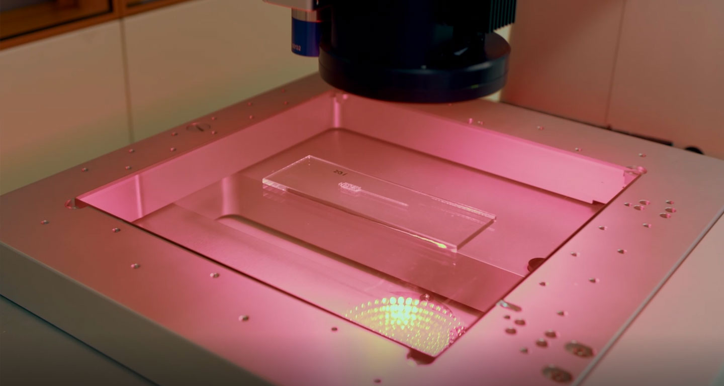
The core FEMTOPRINT® platform integrates ultrafast laser exposure with advanced chemical wet etching. This subtractive process allows for the creation of monolithic, three-dimensional glass devices with unmatched micrometric resolution.
What 3D glass microfabrication capabilities does the FEMTOPRINT® platform enable?
Our Core Capabilities:
What complementary services does FEMTOPRINT offer alongside the core laser platform?
Vertical Integration & Turnkey Solutions: We provide a full-spectrum vertical integration strategy to deliver ready-to-use, tested glass microsystems. Our end-to-end services include:
These services include:
Combining our advanced laser technology platform with standard industrial processes and traceability data, we manufacture ready-to-use products.
What makes FEMTOPRINT's technology fundamentally different from conventional glass microfabrication?
Conventional glass microfabrication, photolithography followed by HF wet etching, sandblasting, mechanical drilling, or laser ablation, is a surface process. It creates 2D patterns at the glass surface or 2.5D depth profiles limited by isotropic etch geometry. It requires photomasks, photoresist, cleanroom environments, and multi-step alignment between separately processed layers when three-dimensional features are needed.
FEMTOPRINT's femtosecond laser selective etching (SLE) is volumetric. The modification, and therefore the etched geometry, exists anywhere inside the glass bulk, at any depth, in any three-dimensional configuration, defined purely by where the laser focus was positioned. No surface access is required. No mask defines the geometry. No layer-by-layer stacking builds the third dimension.
The practical consequences for device designers are fundamental:
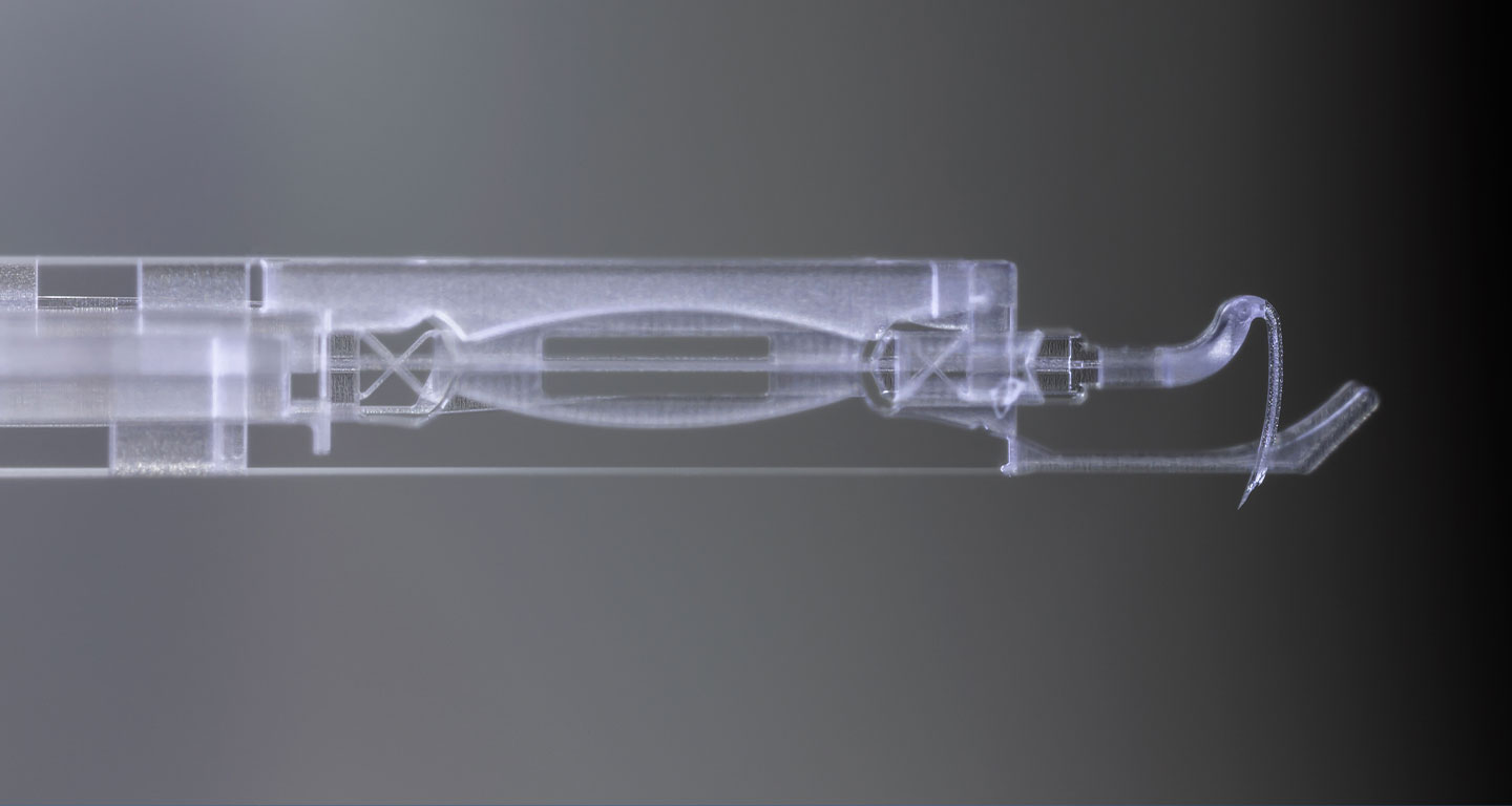
Buried channels can cross each other in three dimensions without intersection, impossible in any planar process. Internal cavities can be created with no external opening, sealed by the surrounding glass. Optical waveguides can be written inside a mechanical structure that simultaneously contains microfluidic channels, co-integrated in one piece without assembly.
We do this according to the most stringent quality requirements to achieve the highest possible output.
 Maskless technology, ensuring fast turnaround cycles in prototyping
3D microfabrication in a monolithic fashion, avoiding costly alignment and assembly steps
Suitable for a large spectrum of glass families
3D shape accuracy ≈ 1µm
Aspect ratio >> 1:500
Min feature size: 2 µm
Max working area: 200x200mm
Max. / min. substrate thickness: 32 mm / 30 µm
Maskless technology, ensuring fast turnaround cycles in prototyping
3D microfabrication in a monolithic fashion, avoiding costly alignment and assembly steps
Suitable for a large spectrum of glass families
3D shape accuracy ≈ 1µm
Aspect ratio >> 1:500
Min feature size: 2 µm
Max working area: 200x200mm
Max. / min. substrate thickness: 32 mm / 30 µm