The researchers showcase multi-material 3D microprinting of wafer scale chips using the unique FEMTOPRINT® microfabrication platform for precise 3D structuring in fused silica glass (SiO2) and selective silicon nitride ablation, in parallel to low-pressure chemical vapor deposition (LPVCD) of silicon nitride (SiNx). This novel procedure leads to a freestanding SiNx window, which is permanently attached to a SiO2 support chip. After parallel chip manufacturing, the researchers created a single nanopore in each chip by focused helium-ion beam or by controlled breakdown (CBD). Compared to silicon chips, the resulting fused silica nanopore chips resulted in a 4-fold improvement of both the signal-to-noise ratio and the capture rate for signals from the translocation of IgG1 proteins at a recording bandwidth of 50 kHz. At a bandwidth of ~1 MHz, the noise from the fused silica nanopore chips was 3- to 6-fold reduced compared to silicon chips. In contrast to silicon chips, fused silica chips showed no laser-induced current noise – a significant benefit for experiments that strive to combine nanopore-based electrical and optical measurements.
Resistive pulse sensing with solid-state nanopores enables characterization of single biomolecules such as DNA, RNA, proteins and carbohydrates. For these experiments, a single nanopore in an ionically insulating substrate is placed between two reservoirs that are filled with electrolyte solution. An electrical potential difference applied between electrodes in these two reservoirs leads to a steady state ionic baseline current through this nanopore. When an insulating particle such as a biological macromolecule passes through the pore, it transiently reduces the ionic current and produces a ‘resistive pulse’ that contains rich information about the physical properties of the biomolecule. Because the strong (MV/m) electric field in the nanopore moves charged particles and proteins through the pore on time scales of nano- to milliseconds, the temporal resolution of resistive pulse recordings is one of the most important and limiting parameters of the technique.
In order to resolve globular macromolecules passing through nanopores on time scales of nano- and microseconds, high-bandwidth recordings with low levels of recording noise are required, with bandwidths beginning at 50 kHz and ideally approaching 1 to 10 MHz. Resistive pulse sensing with nanopores suffers from four major contributions to noise, namely flicker noise, thermal noise, dielectric noise, and amplifier noise (these last ones being the main noise sources that become increasingly important for high bandwidth recordings).
Chips with nanopores for resistive pulse sensing usually consist of a support material with a cavity on one side, which leads to a freestanding membrane containing a nanopore. The support material is usually silicon based, however, due to the semi-conducting electrical properties and the presence of thin, insulating SiO2 or SiNx layers on many silicon support structures, silicon chips can have a large capacitance, leading to large current noise at high recording bandwidth. Nonetheless, silicon remained the material of choice due to its established manufacturability, until researchers approached the FEMTOPRINT® technology, capable of creating sub-micrometer features for high volume production of 3D structured devices.
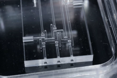
The multi-material fabrication process takes advantage of SiO2 because of its transition temperature of around 1200 °C, the dielectric properties and making it possible to carry out LPCVD of SiNx at 800 °C. 322 chips have been fabricated on a 100mm diameter wafer (Figure 1b). The dimensions of the chips were 4 mm × 4 mm with a thickness of 500 μm. Figure 1d shows the freestanding SiNx membrane with diameters ranging from 5 to 40 μm and corresponding surface areas between 20 to 1250 μm2. The FEMTOPRINT® technology, entirely mask- and cleanroom-free, reduced the number of processing steps. By directly patterning and etching both the cavity and break lines into the wafer along the edges of the chips, FEMTOPRINT separated the chips from the wafer without dicing. This approach thus circumvents vibrations and pressure gradients from a waterjet for cooling the diamond blade during dicing and may be beneficial for processing chips with extremely fragile freestanding membranes or membranes with fragile surface features. Moreover, the 3D patterning and accelerated etching may enable future designs with lab-on-a-chip type microfluidic configurations in fused silica chips. For instance, it is straightforward to integrate fluidic channels within bulk silica material.
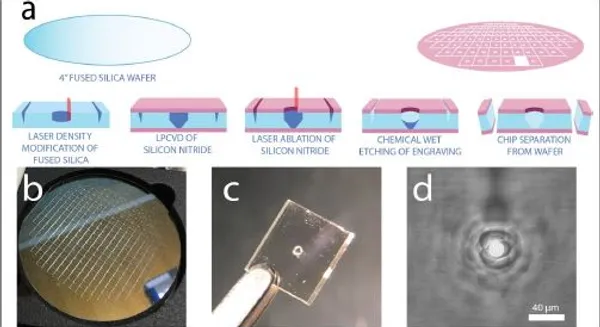
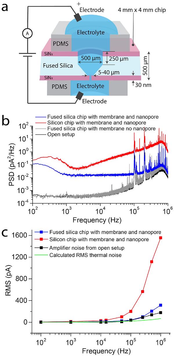
Figure 2 illustrates that the power spectral density (PSD) from the current measured with a fused silica chip with a closed membrane was only slightly larger than the PSD from the open setup over the entire bandwidth range. This result reveals that the fused silica chips presented here made it possible to record close to the lowest noise limit of our recording setup and configuration.
Fabricating a nanopore in these membranes led to the contribution of an additional source of noise to the total current noise. The fused silica chips developed here, as well as other chips with a capacitance below 1 pF, provide at least a 3-fold reduction of noise levels at all bandwidths and become increasingly beneficial at high recording bandwidths. The insulating properties of the bulk material of the fused silica and concomitant reduction in capacitance made these chips particularly suitable for low-noise resistive pulse sensing at high recording bandwidths.
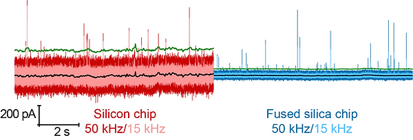
In the context of resistive pulse recordings, the noise level of the current baseline in combination with the length and diameter of the nanopore determines the minimum detectable volume of the biomolecule. As proteins can translocate through a nanopore on a timescale of microseconds or less, resistive pulses should ideally be recorded at bandwidths of at least 1 MHz to resolve most resistive pulses. Figure 3 compares current versus time recordings from translocations of IgG1 proteins through a nanopore and shows, along with Figure 2c, that the noise in the bandwidth range from 15 kHz to 50 kHz from the fused silica chip was 4-fold lower than the noise from the silicon chip. The IgG1 proteins are non-spherical and therefore – as we showed previously – the peak amplitudes in the recorded current vary depending on the shape and orientation of the proteins during their passage through the pore. Moreover, the SNR of the fused silica chip was at least 3.6-fold greater than the silicon chip when both recordings were filtered at 50 kHz.
This research introduced a unique multi-material fabrication process of 3D structuring in SiO2 combined with SiNx deposition and selective ablation, making possible the permanently attached and freestanding SiNx membrane on a wafer scale, reducing fabrication complexity and costs. These chips improve the signal-to-noise ratio of electrical recordings four-fold when compared to silicon chips that have similar geometrical properties. Application wise, the project shows that improvements in the recorded current noise provide a range of practical benefits in the context of protein sensing with nanopores. For instance, nanopores in fused silica substrates make it possible to detect and characterize protein translocation events at 4-fold higher frequency than nanopores in silicon substrates, enabling label-free biomolecule detection with improved statistics. In combination with recent developments in integrated CMOS current amplifiers, these low-noise chips could further improve the information content and accuracy of estimates of multiple parameters calculated from the resistive pulses of individual globular biomolecules such as proteins.
Additionally, the fused silica substrates prepared here showed no laser-induced electrical noise upon illumination. In contrast, measurements with silicon chips showed strong noise upon laser illumination in agreement with a previous report. Therefore, fused silica substrates are well suited for nanopore-based experiments that perform electrical recording and optical monitoring in parallel.
The FEMTOPRINT® technology has potential benefits extending beyond producing nanopores, as it can generate other three-dimensional nanoscale features such as fluidic channels, mixers and reaction chambers on the surface or within the transparent bulk material of fused silica. Integrating fused silica-based substrates with 2D materials like graphene, hexagonal boron nitride, or molybdenum disulfide (MoS2), may reduce the dielectric noise in 3D material-based nanopore recordings compared to supporting these materials on silicon chips. These kinds of nanopore chips have attracted broad interest due to their spatial resolution in DNA sequencing but have been limited by high frequency noise. Advanced combinations of these lab-on-a-chip features with nanopore detectors, produced in a batch format, may ultimately enable the next generation of nano- and microscale devices with possible applications in low-cost diagnostics, point-of-care devices, fundamental biophysics studies, and implantable measurement systems. Moreover, in the context of recent work on large area nanopore arrays, the direct writing method presented here may contribute to the field of energy research where such arrays in membranes function as part of energy storage or conversion devices.
ACKNOWLEDGEMENTS
FEMTOPRINT thanks the authors of this work, which has been published on Nanotechnology Journal.