Since the early 90’s, microfluidics is gaining visibility thanks to the cross-contamination of emerging microfabrication technologies, in particular started within the microelectronics industry. Photolithography techniques, and later etching procedures, gave birth to the first integrated circuits, microprocessors and finally MEMS, being then widely adopted for the fabrication of microfluidic lab-on-chips. Today, the interest is not limited only at experimental level, with a transition to an important market projected at USD 8.78Bi. by 2021 and with a CAGR of 19.2% (2016-2021) (www.marketsandmarkets.com). Concrete industrial applications are disseminated in many fields such as genomics, flow chemistry, and real-time screenings for Point-of-Care diagnostics, which require a certain level of standardization when it comes to mass production, quality assurance and integration into other products.
The work currently conducted under the MFManufacturing project (www.mf-manufacturing.eu) is focusing on building the appropriate terminology, getting minimal requirements for chip size, ports position, diameter and nomenclature, and finally setting the guidelines for the correct designing of new microfluidic sensors, actuators and connectors to facilitate the integration with other microfluidic components or systems.
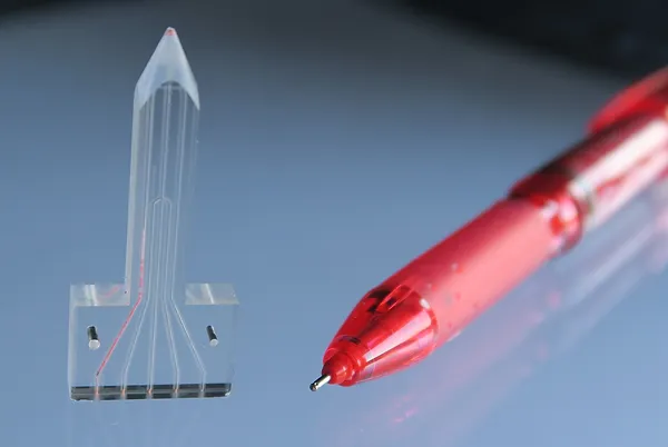
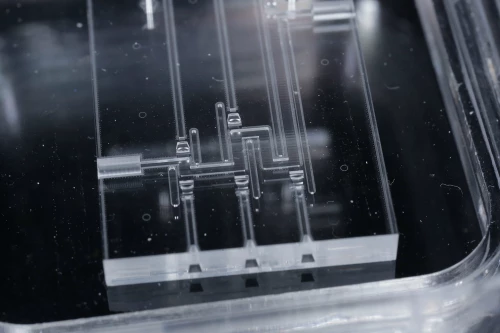
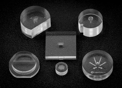
The FEMTOPRINT® technology, based on a two-step process of ultrashort pulsed laser radiation in transparent materials, followed by chemical wet etching to selectively remove the exposed material, is gaining important visibility in this segment thanks to its capability of creating free forms in three dimensions, the exceptional micrometric resolution and the compatibility to industrial standards for large volumes throughput (the company is also ISO 13485:2016 certified).
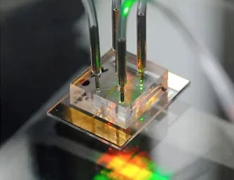
While customers could benefit from standardizations to reduce costs, get higher quality products and fasten the integration with other components, our novel technology is giving the opportunity to engineers to explore the third dimension, add feature-sized complexity and integrate optical, mechanical, physical or even electrical functionalities to the microfluidic device, resulting in higher performances and disruptive applications in single glass monoliths. Deposition of metals to create embedded electrodes, surface functionalization to form hydrophobic or hydrophilic surfaces, or coupling waveguides to structure optofluidic devices are some of the examples of integration in glass lab-on-chips. Further beyond standardization aspects, more sophisticated devices, operating at high temperature above 80°C and with a maximum pressure above 40 bars, benefit from glass exceptional resistance to heat and stress. This is also true for microfluidic devices exceeding the standard microscopy slide size of 26mm x 76mm, where our low-temperature manufacturing platform allows the fabrication of leaktight lab-on-chips with an alignment precision of 2 microns and geometrical precision of 1 micron. The result is a glue- and chemical-free process, avoiding imaging loss of quality and sample contamination. Finally, space limited applications could also benefit from the integration of connection ports directly into the microfluidic chip, following at the same time the standardization guidelines as per port size, positioning and port coding. In this case the technology offers the possibility to create monolithic ports directly into the chip, flat, coned or in any other shape, perfectly matching the hollow screw fittings broadly available in the market with a precision below 5 microns along the depth.

To conclude, the FEMTOPRINT® 3D printing technology is an industrial reality also for microfluidics, allowing users to boost even more the limits of creativity and the performance of their chips, giving birth to true innovative solutions which find nowadays tangible industrial opportunities. In this context, standardization is a fundamental step towards this even more challenging, qualitative and cost-effective sector, benefitting all stakeholders, from foundries to consumers, and of great support to set solid basis for innovative solutions to come.