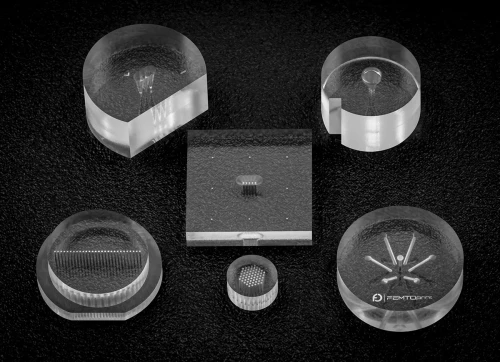
At FEMTOPRINT, we specialize in high-precision glass microfabrication using femtosecond lasers. Our platform allows custom fabrication of monolithic ion traps in fused silica with sub-micron accuracy—ideal for scalable and fault-tolerant quantum processor architectures.
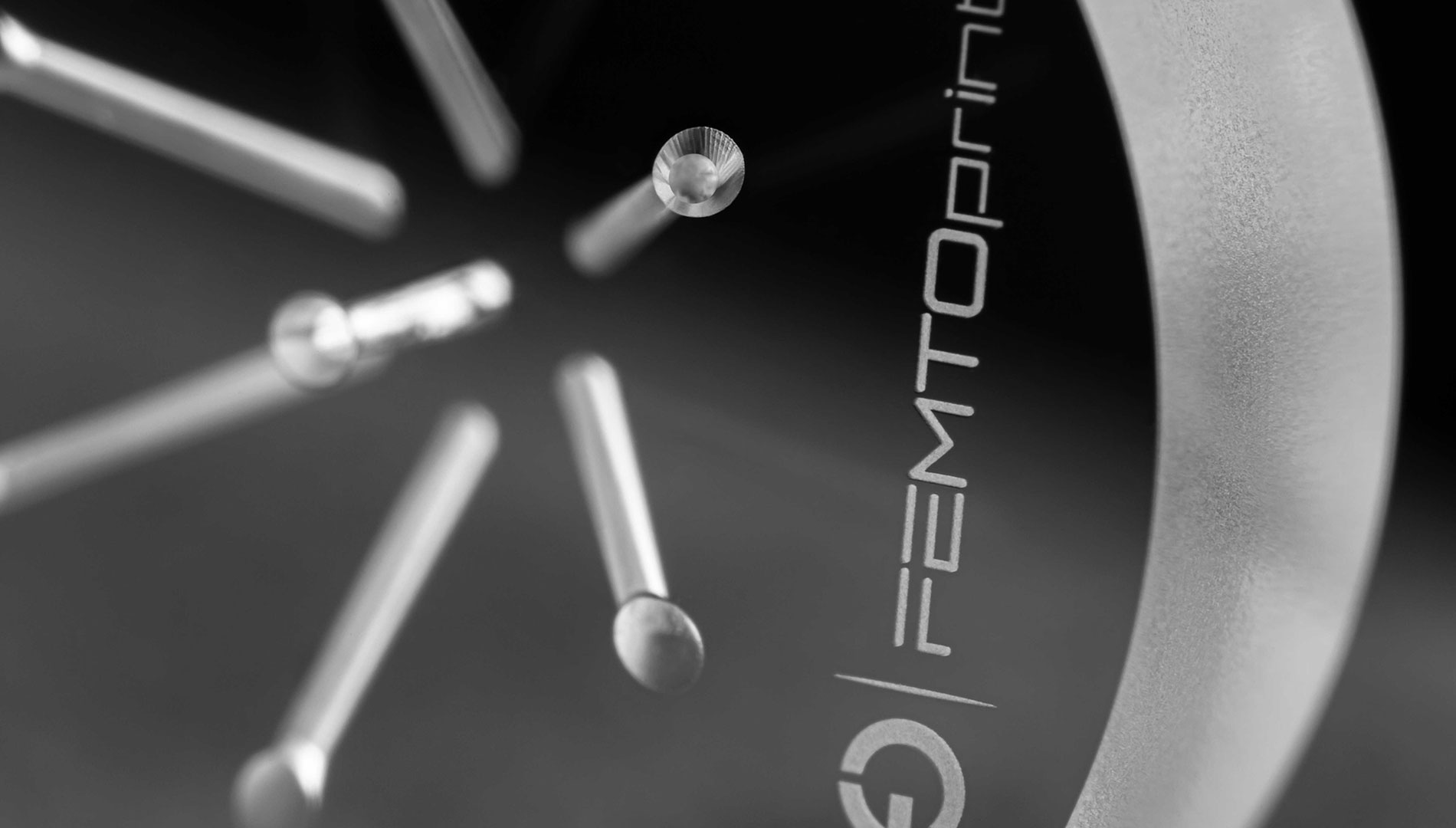
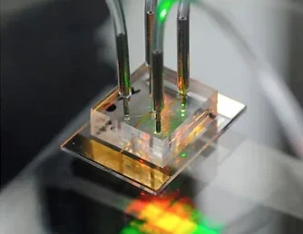
FEMTOPRINT fabricates 3D ion traps as a single monolithic block of fused silica, shaped in three dimensions by femtosecond laser and selective laser etching (SLE). No stacked wafers, no bonding, no spacer. One piece of glass with the trap geometry written directly inside it. For trapped-ion quantum processors, that removes a failure mode the field has lived with for years.
Surface (planar) traps are easy to microfabricate, which is why they dominate. But the ions sit above an open electrode plane, and the trapping field that results is shallower and less symmetric than a true three-dimensional geometry. 3D traps put electrodes around the ion, not just beneath it. The payoff is deeper trapping potentials, tighter confinement, and lower heating, the conditions that keep qubits coherent long enough to compute.
The catch has always been making the 3D structure without giving back what you gained.That's where the fabrication route matters.
The common way to build a 3D trap is to pattern electrodes on two wafers and bond them around a spacer. It works, but bonding introduces a stack-up tolerance; published multi-wafer traps report alignment on the order of a couple of microns of standard deviation across the stack. Every bonded interface is also a surface where charge can accumulate and contribute to motional heating.
A monolithic trap has neither problem. Because the geometry is written into one fused-silica substrate, there is no inter-wafer alignment to control and no internal bond line. You get the field symmetry of a 3D design without the assembly error that usually comes with it. For a buyer chasing low heating rates and reproducible trap depth across a production run, that's the difference that matters.
Verified process figures (same platform as our wheel traps and Paul traps):
|
Parameter |
Value |
|
Material |
Monolithic fused silica |
|
Process |
Femtosecond laser + selective laser etching (SLE), maskless |
|
Resolution |
~1 µm |
|
Surface roughness |
Sa ≤ 10 nm |
|
Aspect ratio |
≥ 1:500 |
|
Format |
Wafer scale, up to Ø 300 mm |
|
Quality system |
ISO 9001 & ISO 13485 |
Trap-specific parameters, electrode gap, trap depth, RF electrode layout, and metallization scheme are defined per application through a feasibility review, not quoted off the shelf. Every trapped-ion architecture asks for something different, and we'd rather size it to your design than publish a number that doesn't fit it.
Most quantum groups come to us with a design that works on the bench and a scaling problem behind it: how do you go from a handful of hand-finished traps to hundreds of reproducible ones? Because the geometry is laser-written and maskless, the same file that makes your prototype makes the production part, with no new tooling between the two. We run design-for-manufacturing early, so the move from first article to wafer-scale volume doesn't restart the process.
A trap rarely ships alone. We fabricate the electrical and photonic interconnect around it in the same glass platform , photonic connectivity for laser routing and readout, electrical connectivity through TGVs, and glass interposers for hybrid trapped-ion modules. If your roadmap points toward chiplet-style integration, the substrate is already the right one.
A single monolithic block of fused silica. There are no bonded wafers and no internal spacer, so there's no bond line inside the trap.
By femtosecond laser direct writing followed by selective laser etching (SLE). The process is maskless and writes the 3D geometry directly into the glass at roughly 1 µm resolution.
Bonding two patterned wafers around a spacer adds an alignment tolerance and an internal interface where charge can build up. A monolithic trap removes both, which helps with field symmetry and motional heating.
Yes. The process supports free-form 3D geometries and runs at wafer scale up to Ø 300 mm. Because it's maskless, the same design moves from prototype to production without retooling. Trap-specific parameters are defined per application via a feasibility review.
Fused silica is a low-loss dielectric used in ultra-high-vacuum and cryogenic systems. Exact suitability is confirmed per application during the feasibility review.
Speak with our team to develop customized 3D ion traps for your quantum computing applications!
Key Features
Why It Matters
 "We used FEMTOPRINT’s platform to fabricate custom all-glass preforms for Laser Written Vapor Cells (LWVCs), a patented technology exclusively licensed to QSENSATO for Quantum Sensing and Metrology applications. The technical support was continuous, the lead time respected and the micrometric tolerances have been precisely met. The results completely matched our high expectations." Gianvito Lucivero CEO & Founder