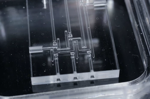
Glass offers a unique combination of high dielectric strength, electromagnetic inertness, and a low/adjustable Coefficient of Thermal Expansion (CTE). Its vacuum compatibility, superior optical access, and sub-micron dimensional precision make it the gold standard for fabricating ion traps, vapor cells, and neutral atom enclosures.
Our platform delivers sub-micron accuracy, which is essential for ensuring stable electric fields and reliable particle confinement. This precision allows us to define ultra-fine structures, including electrodes, trenches, and 3D geometries, with absolute repeatability.
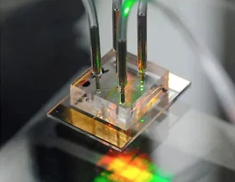
Yes. We specialize in hybrid quantum architectures where refractive optics (mirrors or lenses) coexist with metallized features. Furthermore, we can integrate 3D laser-inscribed waveguides for beam routing. While currently optimized for telecom C-band, we are actively extending our waveguide capabilities to specific quantum wavelengths, including 1760 nm, 700–800 nm, and 400–500 nm.
We utilize advanced laser welding to provide robust, leak-free encapsulation. Currently, our laser welding process is performed at ambient pressure; however, we are in the advanced stages of developing a welding process optimized for Ultra-High Vacuum (UHV) environments.
Fused silica is the preferred material due to its exceptional optical performance, negligible birefringence, and excellent thermal stability, which is critical for reliable operation at cryogenic temperatures.
Yes. Through femtosecond laser drilling and etching, we create precise TGVs. With our integrated metal deposition processes, these vias can be made conductive, achieving sub-Ohm resistance for efficient signal routing in 3D architectures.
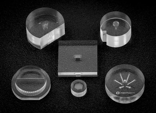
Yes. Our 3D microfabrication capabilities allow for the creation of integrated resonators and optical cavities directly within the monolithic glass substrate, ensuring perfect alignment and stability.
Absolutely. Fused silica maintains excellent mechanical and optical stability under cryogenic conditions, making it ideal for quantum processors and sensors operating at millikelvin temperatures.
Ultra-smooth surfaces are vital in quantum applications to minimize scattering in optical paths and reduce electric field noise, which can otherwise interfere with qubit coherence. We deliver surface finishes tailored to these stringent requirements.
Yes. Our platform supports batch processing on glass substrates, enabling the scalable production of array-based systems and the transition from laboratory experiments to commercialized quantum hardware.
Do you have any other questions? Talk to our expert