Glass provides exceptional optical transparency and low propagation loss.Its thermal expansion coefficient is highly compatible with optical fibers, and its unique structure allows for high-precision 3D waveguide inscription, making it the superior choice for high-density interconnects.
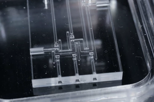
Yes. Using Femtosecond Laser Direct Writing (FLDW), we can create complex 3D waveguides directly inside the glass. This allows for multi-layer optical routing and true 3D photonic integrated circuits (PICs) that are impossible with traditional 2D lithography.
Our glass-based photonics typically support a broad spectrum from UV to Near-IR. While our waveguides are frequently optimized for C-band and L-band (Near-IR) for telecommunications, we can also develop custom fabrication processes for Visible (VIS) light applications.
Extremely. Glass maintains a consistent refractive index and geometric stability even under high-temperature operations. This thermal robustness is critical for maintaining optical alignment in high-power laser systems and co-packaged optics.
We achieve micrometer-level positional accuracy. This high precision is fundamental to ensuring low insertion loss and optimized mode-field matching when coupling light between fibers, waveguides, and active components.
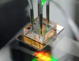
Yes. Through our vertical integration, we combine 3D optical routing with precision metallization. This enables hybrid opto-electronic integration, allowing electrodes and sensors to operate alongside optical waveguides in a monolithic device.
To minimize scattering and optical loss, we deliver surface roughness levels from 50nm down to < 10nm Ra. This ultra-smooth finish is essential for high-Q resonators and low-loss waveguides.
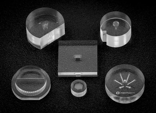
Absolutely. We fabricate high-precision glass ferrules, including V-grooves and complex 1D/2D hole arrays. These can be seamlessly combined with micro-optics and waveguides within the same substrate for automated, low-loss fiber alignment.
Our technology is designed for the entire product lifecycle. Our wafer-level production allows customers to move seamlessly from rapid prototyping to mass manufacturing, ensuring consistent quality and cost-efficiency at scale.
Our solutions power the most demanding sectors, including Data Centers (Data-/Tele-com), Co-Packaged Optics (CPO), Photonic Computing, Quantum Optics, and advanced sensing for Aerospace and Defense.
Discover More. Contact Us Today!