In industries requiring micron-level precision—such as photonics, medical devices, and microfluidics—the ability to rapidly prototype and validate glass-based components is critical. FEMTOPRINT SA’s integrated approach to glass microfabrication combines advanced techniques like 3D shaping, waveguide patterning, and wafer-scale manufacturing to address the limitations of traditional prototyping methods.
By merging multidisciplinary expertise in material science, optics, and industrialized technology, we demonstrate how seamless scalability from concept to mass production can reduce development cycles while ensuring high-accuracy outcomes.
The Challenge of Modern Prototyping
The demand for miniaturized, high-performance glass components—used in optical systems, biosensors, and quantum technologies—has intensified. However, conventional processes like lithography often struggle with speed, cost, and geometric complexity. Prototyping delays directly impact time-to-market, creating a need for agile, precision-driven solutions.
FEMTOPRINT SA bridges this gap through a full-stack prototyping framework tailored for glass substrates. Our methodology prioritizes:
Technical Framework: Core Capabilities
1. High-Accuracy Fabrication Processes
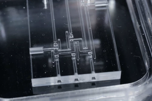
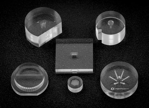
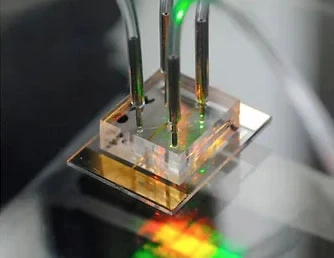
Our platform leverages femtosecond laser-based 3D shaping to create complex geometries within bulk glass, bypassing layer-by-layer additive manufacturing constraints. Key processes include:
2. Multidisciplinary Optimization
Cross-domain expertise in physics and material science enables predictive modeling and simulation of thermal, mechanical, and optical behaviours. This reduces trial-and-error cycles, ensuring prototypes meet functional requirements from the first iteration.
3. Industrialized Workflow
Unlike academic or artisanal approaches, our wafer-scale manufacturing platform standardizes processes across 100+ mm glass substrates. This ensures consistency, reduces unit costs, and simplifies transitions to large-scale production.
Advantages Over Traditional Methods
Eliminating Bottlenecks
By integrating project management tools with real-time process monitoring, we mitigate risks of misalignment between design and fabrication, a common issue in multi-vendor workflows.
Cost Efficiency
Wafer-scale processing reduces material waste by 30%, while standardized protocols minimize post-fabrication adjustments.
The fusion of high-accuracy glass microfabrication with industrialized workflows offers a paradigm shift in prototyping efficiency. As industries push toward smaller, smarter devices, FEMTOPRINT SA’s single-source model—combining R&D agility with production robustness—positions it as a critical partner for innovation.
Explore our technical portfolio or discuss a project with our engineering Team, today.