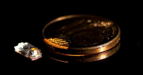
From 21 to 23 September 2026 at FYCMA, Málaga. You will find our team at booth 1419.
ECOC is Europe's largest optical communications event and the second largest worldwide, drawing more than 8,000 industry attendees and over 340 exhibitors. For a Swiss CDMO working in 3D glass microfabrication, it is the one week of the year when the entire fiber, datacom and integrated photonics supply chain is in the same building.
This year we are bringing one specific conversation to Málaga: what happens to your optical packaging when the alignment features, the micro-optics and the waveguides all live inside a single piece of glass.
Why photonic integration keeps hitting the same wall
Every optical link budget has a section nobody enjoys reviewing: the losses that come from interfaces rather than from physics.
Each transition between fiber and chip introduces an interface. Each interface introduces insertion loss, an alignment tolerance and a mechanical failure mode. Polymer and epoxy-based alignment structures drift across the temperature swings of a data center rack. Assembled sub-components stack their tolerances until active alignment becomes the only way to hit the spec — and active alignment does not scale to the channel counts that co-packaged optics and AI cluster interconnects now demand.
The usual answer is to tighten the assembly process. The alternative is to remove assembly steps entirely.
What we do differently: monolithic 3D glass microfabrication
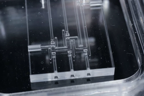
FEMTOPRINT uses selective laser etching (SLE): a femtosecond laser is focused inside a fused silica or borosilicate substrate, locally modifying the material through non-linear absorption. The exposed regions etch far faster than the surrounding glass, so a true three-dimensional geometry can be developed inside a solid block.
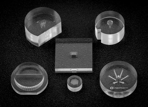
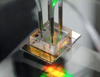
The process is maskless and volumetric. Buried channels, undercuts, curved internal surfaces, fiber-alignment features, micro-optical elements, and optical waveguides can be produced in the same monolithic part—no photomasks, no cleanroom lithography, no bonded layers, no adhesives in the optical path.
For photonic packaging, that changes the arithmetic. A lens, a buried waveguide, and a fiber ferrule fabricated as one piece of glass have no alignment tolerance stack between them, because there is nothing to align.
What our experts will discuss at booth 1419
3 main topics are on the table.
We will also be talking about scale. The same process that produces a single prototype runs at wafer level up to 300 mm, under ISO 9001:2015 and ISO 13485:2016, which matters when the question stops being "can this be built" and becomes "can this be built ten thousand times.
Book a meeting before the floor fills up
Booth slots at ECOC go quickly, and the most useful conversations are the ones with a drawing on the table. Send us your design or your optical layout ahead of the show and we will come to the meeting with a feasibility answer, not a brochure.
Frequently asked questions
Where and when is ECOC 2026? ECOC 2026 takes place at FYCMA in Málaga, Spain. The exhibition runs 21–23 September 2026 and the conference runs 20–24 September 2026.
Where is FEMTOPRINT at ECOC 2026? FEMTOPRINT is at booth 1419.
What is FEMTOPRINT showing at ECOC 2026? Custom 3D glass micro-optics and buried waveguides for fiber-to-chip coupling, high-precision glass ferrules and high-aspect-ratio microstructures, and monolithic designs that reduce assembly steps in photonic packaging.
What is selective laser etching (SLE)? A two-stage process in which a femtosecond laser modifies glass in three dimensions inside the bulk material, after which a chemical etch removes the modified regions far faster than the untouched glass. It is maskless and produces true 3D geometries in a single monolithic substrate.
Which glass materials can FEMTOPRINT process? Fused silica, fused quartz, borosilicate including Borofloat® 33, aluminosilicate, alkali-free glasses and ULE. Material selection for a given application is defined during feasibility review.
Can FEMTOPRINT scale from prototype to volume production? Yes. The same process runs from single prototypes to wafer-level batches on substrates up to 300 mm, under ISO 9001:2015 and ISO 13485:2016.