If your engineering organization is designing next-generation AI clusters, high-performance computing (HPC) nodes, or hyperscale data center architectures, you already know the brutal reality: electronic interconnects have hit a physical wall.
To satisfy the immense bandwidth requirements of 800G, 1.6T, and 3.2T architectures, hyperscalers are aggressively transitioning to Co-Packaged Optics (CPO) and high-density pluggable optics. Moving optical transceivers off the front panel and mounting photonic integrated circuits (PICs) directly onto the substrate alongside GPUs or ASICs saves power and slashes latency.
However, a critical hardware bottleneck remains:
What’s consuming your optical link budget before you’ve even started?
It’s the fiber-to-chip interface.
As AI clusters push optical I/O onto the package, every microscopic mis-alignment, mode mismatch, and beam transition quietly drains a power budget that was already razor-thin. When you lose decibels at the coupling interface, you are forced to drive lasers harder, generate unwanted heat, and compromise system-level thermal efficiency.

The Fiber-to-Chip Interface Bottleneck
For Chief Technology Officers (CTOs) and optical system architects across leading US tech hubs—from Silicon Valley and Austin to Boston and Seattle—the physics of fiber-to-chip coupling represent a formidable engineering challenge:
When managing thousands of optical channels across an enterprise AI fabric, sub-optimal coupling is not just an efficiency nuisance—it is a system architecture failure.
3D Waveguide Engineering in Fused Silica
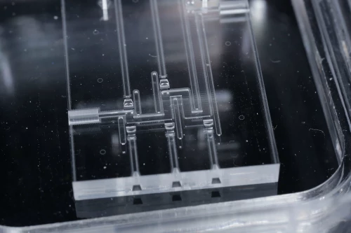
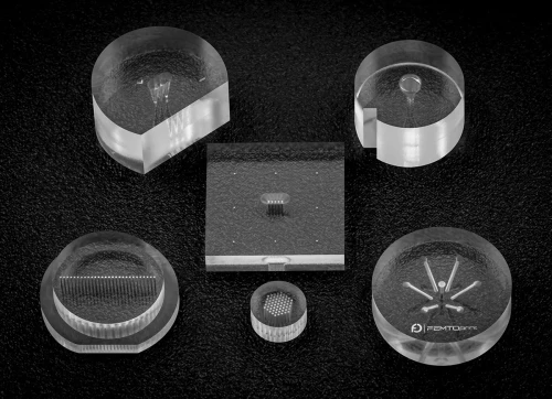
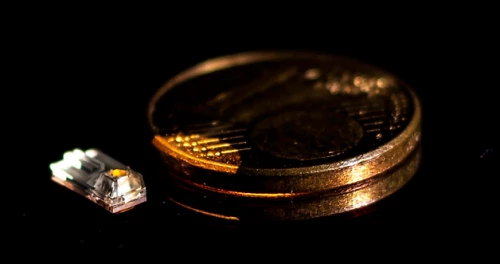
This is where FEMTOPRINT SA shifts the operational curve. Rather than treating the optical interface as a static array of passive fibers, FEMTOPRINT engineers monolithic 3D optical interfaces written directly inside fused silica glass using proprietary ultrafast femtosecond laser micro-machining.
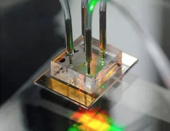
By utilizing high-precision laser direct-writing, FEMTOPRINT enables 3D volumetric light routing, seamlessly transforming signal topographies between optical fibers and photonic integrated circuits.
Key Performance Metrics for Engineers and Architects

Reproducibility at Industrial Volume
In high-speed optical networking, producing a single ideal prototype is only a starting point:
The hard part was never the first waveguide. It’s the ten-thousandth one performing exactly like the first one.
By eliminating traditional assembly-based multi-part optics in favor of a monolithic glass substrate, FEMTOPRINT delivers sub-micron repeatability across millions of optical channels. Explore how our proprietary 3D glass optical waveguides for PICs and interconnects redefine density, structural stability, and thermal resilience.
Recover Your Optical Link Budget Today
Where is your fiber-to-chip coupling budget going in your current CPO and pluggable optics designs? Stop sacrificing optical power to interface friction.
Whether your R&D team is scaling silicon photonics transceivers, building next-generation quantum computing optical backplanes, or optimizing thermal envelopes for AI accelerators, FEMTOPRINT provides end-to-end engineering—from initial feasibility and rapid prototyping to full wafer-scale industrial production.
Take the Next Step
Discover more, speak with our expert.