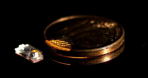
What's new is what sits next to those electrodes: waveguides, fiber slots, and free-form optics, cut into the same block of glass, in the same fabrication run.
At a recent quantum photonics conference, Cesare Alfieri, Business Developer Quantum at FEMTOPRINT, walked through how this works, and why it matters for anyone building ion trap hardware that needs to scale past a handful of qubits. The short version: no separate photonic chip to bond, no fiber array to hand-align under a microscope, no adhesive joint to fail during a bake-out, no second vendor in the loop. The optics come out of the glass already positioned.
This is photonic connectivity built into the trap, not stacked on top of it.
Most ion trap papers focus on electrode geometry, RF drive, and coherence times. Fewer talk about what happens after the trap is built: getting light in and out of it.
The standard route is bulk optics, lenses and mirrors on an external breadboard, aimed through vacuum windows at ions trapped 50-100 µm above a chip surface. It works in a lab. It doesn't scale. Every extra optical path is another source of drift, another alignment to redo after a thermal cycle.
The next step, and the one most of the field is chasing, is photonic integration: routing light on-chip instead of through free space. Recent published work on silicon nitride photonic integrated circuits (PICs) bonded to surface-electrode traps shows the appeal, and the catch. You still need to align and bond a separate PIC die to the trap substrate. That's one more interface, one more CTE mismatch to manage at cryogenic temperatures.
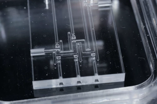
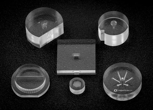
Monolithic photonic connectivity means the waveguides, fiber slots, and free-form optics exist inside the same piece of fused silica as the trap electrodes, fabricated in one continuous process. There's no PIC die to bond, no separate optical bench, no post-assembly alignment step. Light enters through a fiber slot cut directly into the glass, travels through a laser-written waveguide, and exits through a free-form micro-optic — all positioned by the same process that shaped the trap itself.
FEMTOPRINT builds this with Selective Laser Etching (SLE): a femtosecond laser modifies the glass in three dimensions, then a selective etch removes the modified material, leaving trenches, channels, and buried optical paths in one substrate. Because everything comes from a single writing step, the relative position of a fiber slot to a waveguide to an electrode is fixed by the laser's positioning accuracy, not by how well a technician can align two separate parts under a microscope afterward.
Any of these can be combined in a single part. None of them requires a second fabrication step or a second vendor.
For anyone specifying tolerances on an RFQ, here's what's achievable in fused silica on FEMTOPRINT's platform:
|
Parameter |
Value |
|
XY positioning |
± 1 µm |
|
Z positioning |
± 2 µm |
|
Surface roughness after treatment (Sa) |
< 10 nm |
|
Minimum feature size |
< 5 µm |
|
Aspect ratio |
up to 1:500 |
|
Wafer scale |
up to Ø 300 mm |
That surface roughness figure is the one worth sitting with for a second. Ten nanometers isn't a marketing round number. It's the difference between a clean optical surface and one that scatters enough stray light to show up as noise in a sensitive measurement.
A rough surface scatters light. Inside an ion trap, that's not a cosmetic problem: stray light near the trapping region adds background counts to fluorescence detection, and rough surfaces are more prone to the kind of contamination and charge build-up that destabilizes ion confinement. Post-treatment surface roughness below 10 nm Sa keeps optical paths clean. FEMTOPRINT gets there in two steps: patterned surfaces come off the laser process at roughly 100 nm Sa, then a polishing step brings that down to under 10 nm where it matters most.
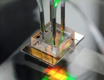
Alfieri's talk walked through a live demonstration: a 3D glass ion trap with waveguides, fiber slots, and free-form optics fabricated directly into the substrate, no assembly step between "fabricated" and "ready to test." For an audience of photonics and quantum hardware engineers, that's the part that gets attention. Most of the room has spent time re-aligning a fiber array after every cool-down. Fewer have seen a trap where that step doesn't exist.
The full presentation, recorded at the conference, covers the fabrication process in more depth than this article can, including the trench geometries and multi-layer structures behind the electrode side of the same trap. Watch the full presentation on integrated optical connectivity for glass quantum devices →
If you're building 3D glass ion traps for quantum computing, quantum simulation, optical atomic clocks, or precision mass spectrometry, and you're past the single-trap stage, looking at multi-zone architectures where every extra optical interface multiplies your alignment budget, this is worth a technical conversation. Substrate thickness runs from under 0.5 mm to over 10 mm; trench designs can include buried structures, overhanging features, and multi-layer stacks alongside the optical paths. Electrical connectivity — metallized trenches and through-glass vias, can be fabricated on the same substrate as the photonics, if your architecture needs both.
Have an ion trap design that needs photonic connectivity built in from the start, not bolted on afterward?
Talk to our expert and the Quantum team, today.
It's the set of optical paths, fiber inputs, waveguides, and beam-shaping optics, that get light into and out of an ion trap. In FEMTOPRINT's process, these are fabricated directly into the glass substrate alongside the trap electrodes, in one process, instead of assembled from separate components afterward.
An assembled approach bonds a separate photonic integrated circuit or fiber array to a trap substrate after both are fabricated, which requires an alignment step and introduces a bonded interface. A monolithic approach fabricates the waveguides, fiber slots, and optics inside the same glass part as the trap itself, so there's no separate piece to align or bond.
XY positioning of ±1 µm and Z positioning of ±2 µm, with surface roughness (Sa) below 10 nm after surface treatment. Minimum feature size is under 5 µm, and aspect ratios up to 1:500 are achievable in fused silica.
Yes. Metallized electrodes (typically gold, titanium, chromium, or platinum) and laser-written optical paths can be fabricated on or in the same substrate, combining electrical and photonic connectivity in one monolithic part.
The full recording is linked above and on FEMTOPRINT's YouTube channel.