With NVIDIA’s recent announcement of its Spectrum-X networking platform, the paradigm shift to silicon photonics, with Photonic Integrated Circuits (PICs) enabling Co-Packaged Optics (CPO) solutions, has taken center stage. As hyperscale data centers evolve into full-scale AI factories, the need for faster, more efficient, and more compact interconnect solutions is skyrocketing.
But behind the scenes of this high-performance optical revolution lies a critical enabler: precision glass microfabrication.
What’s Driving the Shift Toward Silicon Photonics and Co-Packaged Optics?
The combination of PICs and CPO solutions brings the optical engine closer to the switch ASIC, reducing power consumption and latency by eliminating traditional transceivers. This is crucial for the performance demands of Generative AI, High-Performance Computing (HPC), and large-scale machine learning infrastructure.
These new architectures require:
Traditional packaging approaches often fall short—especially when it comes to the precision and form factor required. That’s where glass microfabrication becomes a game-changer.
The Role of Glass in Optical Packaging
Glass is an ideal substrate for advanced photonics applications, offering:
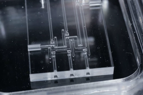
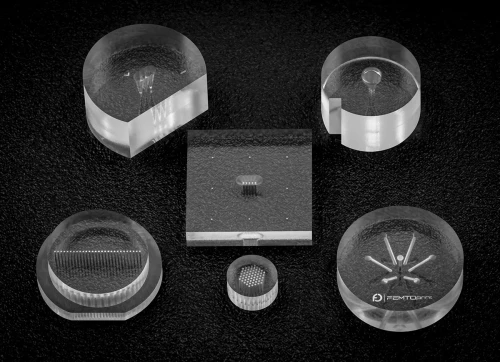
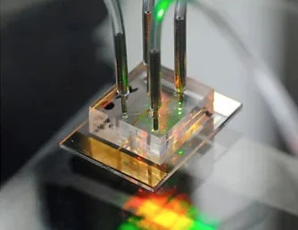
At FEMTOPRINT, we leverage ultrafast femtosecond laser microfabrication to create 3D glass microstructures with sub-micron resolution.
What We Enable:
This is not just prototyping — it’s production-ready performance.
From PICs to AI Factories
As the demand grows for PICsCPO modules, there’s increasing pressure on manufacturers to move quickly from proof-of-concept to production.
Thanks to our monolithic glass structuring, FEMTOPRINT enables customers to:
Shorten the development cycles and rapidly upscale to production volumes. We work directly with companies producing optical engines, fiber assemblies, PIC devices, the new generation of optical transceivers as well as providing packaging and assembly services for the next-generation data centers and AI hardware.
Glass Is the Quiet Hero of Optical Innovation
PICs and CPOs are more than a trend—they represent a true technological leap. And while most of the spotlight is on AI, computing, and switching speeds, the mechanical and optical precision of microfabricated components is just as critical.
At FEMTOPRINT, we’re proud to support the innovators building the future of data infrastructure—one glass microstructure at a time.
Interested in accelerating your roadmap for new photonics devices and innovative optical packaging? Let’s talk.
Co-packaged optics places the photonic integrated circuit on the same package substrate as the switch ASIC, replacing pluggable transceivers. Putting the optical engine next to the chip shortens electrical paths and cuts the power and latency that limit AI-data-center networks.
AI workloads connect huge numbers of GPUs and push bandwidth, power and latency past what copper can sustain. Optical links handle that density, and CPO is the architecture that brings them close enough to the ASIC to matter at scale.
Glass works as an optical interposer and substrate: it carries low-loss embedded waveguides, precise fiber-alignment features and through-glass vias, letting optical and electrical routing share one dimensionally stable, transparent package.
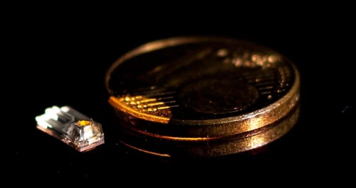
Aligning a single-mode fiber to a sub-micron waveguide demands extreme precision, and that packaging step is a major share of an optical module's cost. Monolithic glass interconnects that self-align their elements reduce that assembly burden.
A femtosecond-laser platform builds monolithic glass interconnects integrating waveguides, micro-optics and alignment features, self-aligned within ±1 µm, at wafer scale up to 300 mm — prototype to volume without re-tooling.