Cookie bar

We use cookies and other tracking technologies to improve your experience and analyse our website traffic.

Please consult our Privacy Policy for more information.

By clicking on “Accept”, you consent to your data being collected

You can change your cookie settings and disable cookies, except for essential functional ones, at any time.


Functional
Preference
Statistical
Marketing
FEMTOPRINT SA

As Artificial Intelligence (AI) and Machine Learning (ML) workloads scale at an exponential rate, traditional copper-based interconnects are hitting a physical wall.

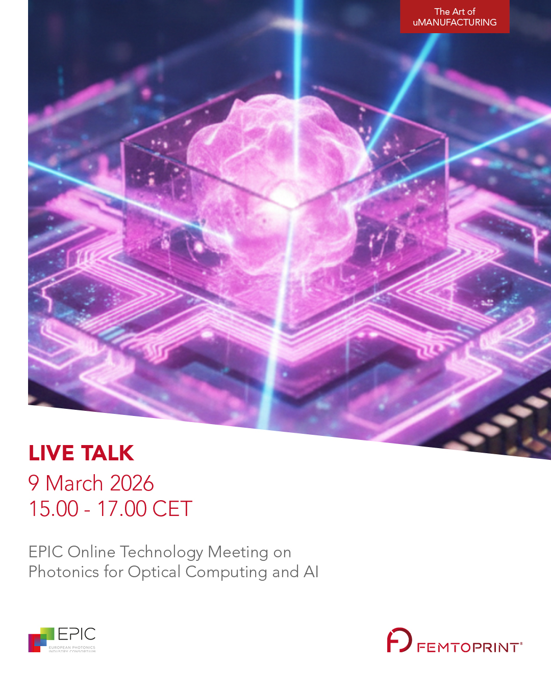
To achieve the next frontier of speed and energy efficiency, the industry is pivoting toward Optical Computing and Photonic Integrated Circuits (PICs).

The primary challenge for next-gen AI hardware is no longer just raw compute power—it is the optical connectivity bottleneck. At the upcoming EPIC (European Photonics Industry Consortium) Tech Meeting, FEMTOPRINT will address how advanced 3D glass micro-components are the key to unlocking the full potential of AI datacenter infrastructure.

Why Glass is the Superior Substrate for Photonic Neural Networks

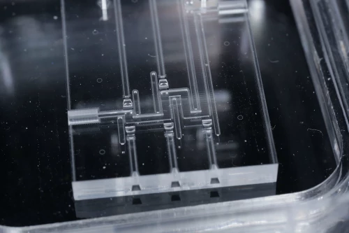
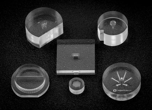
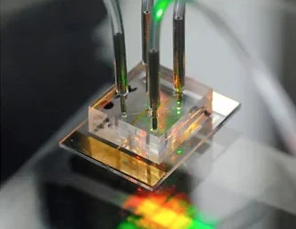
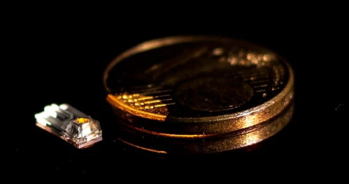
The transition to glass-based substrates is a strategic move for signal integrity. While silicon photonics has provided the foundation, 3D glass micro-fabrication (using high-purity Fused Silica) offers unique advantages to solve the "Power-Performance-Area" challenge:

  • Ultra-Low Insertion Loss: High-precision glass components minimize signal degradation in critical optical interconnects, reducing the need for power-hungry amplifiers.
  • Superior Thermal Management: Unlike polymers, glass maintains unmatched dimensional stability under the intense thermal loads of AI accelerators and GPUs, preventing thermal throttling.
  • True 3D Optical Routing: Our technology enables multi-layer, complex optical paths, moving beyond the density limitations of 2D planar layouts to support Edge AI and massive parallel processing.

Enabling Monolithic Integration for AI Scalability

The path to commercializing Photonic Neural Networks lies in Monolithic Integration. By leveraging our proprietary Femtosecond Laser Micromachining (FLM), we integrate optical, mechanical, and fluidic functions into a single, robust glass substrate. This approach is a game-changer for High-Performance Computing (HPC) because it:

  1. Optimizes SWaP (Size, Weight, and Power): Crucial for high-density, energy-efficient datacenter modules and Co-Packaged Optics (CPO).
  2. Solves Fiber-to-Chip Coupling: Sub-micron precision ensures perfect alignment for light coupling, drastically reducing assembly complexity and latency.
  3. Accelerates R&D Cycles: Our Design-for-Manufacturing (DfM) process allows engineers to move from CAD to functional 3D prototypes in days, reducing the Time-to-Market.


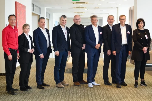
Meet FEMTOPRINT at the EPIC Tech Meeting

The shift toward AI-driven photonics requires a fundamental change in how we manufacture micro-components. Join our talk at the next EPIC event to discover how FEMTOPRINT® technology is providing the hardware backbone for the next generation of on-chip neural networks.

Talk with our expert. TODAY.

Subscribe to our newsletter

Get informed on the latest developments of our company and leading technology!

Sign up now
Contact Us