For CTOs scaling photonic modules from R&D to high-volume manufacturing (HVM), the core issue is clear: packaging costs and yields are eroding margins. As data rates continue their relentless climb, the demand for repeatable, sub-micron alignment tolerances exceeds the capability of conventional mechanical machining and active alignment methodologies. Simply put, when the packaging becomes the bottleneck, your Total Cost of Ownership (TCO) spikes.
Glass: The Deterministic Platform for Integrated Photonics
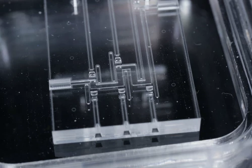
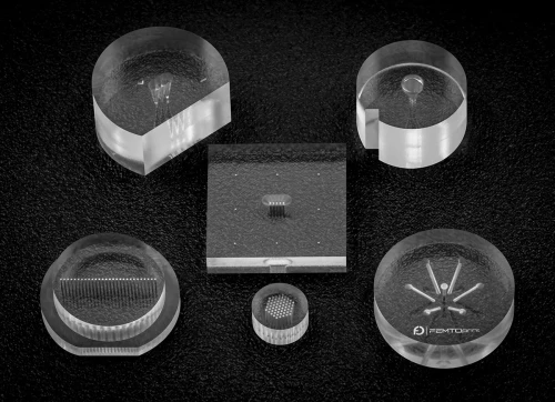
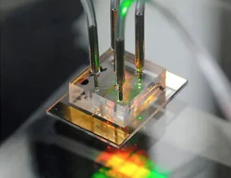
Our upcoming live webinar directly addresses this challenge by presenting 3D laser-structured glass as the solution. Glass is no longer a passive substrate; it is the enabler of performance and scalability for photonic integrated circuits (PICs).
We leverage advanced 3D laser micromachining—specifically, femtosecond laser direct writing—to fabricate precise features directly into the bulk material. This approach bypasses the limitations of traditional CNC processing and ensures performance where it counts:
Strategic Advantage: Define the Next Design Cycle
This presentation is an essential preview of the packaging architecture that will dictate success in the upcoming design cycle. By adopting this technology, you gain a significant competitive edge in Time-to-Market and Cost-Efficiency for demanding applications like AI interconnects and high-speed telecom.