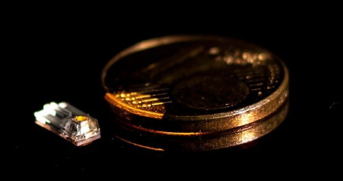
Ask most engineers where quantum computers stall, and they'll point to qubit coherence times, gate fidelity, or error correction overhead. Those are real challenges. But a less-discussed and equally urgent barrier sits at the hardware level, the physical infrastructure that holds, manipulates, and optically addresses qubits at cryogenic temperatures.
Integration and scaling are among the most urgent open problems in quantum computing today. And solving them requires rethinking the materials and fabrication processes used to build quantum hardware from the ground up.
This article explains why glass, specifically monolithic 3D fused silica structures fabricated by femtosecond laser microfabrication, is emerging as a critical enabling material for scalable quantum systems.
3 Hardware Challenges That Block Quantum Scaling
Photonic Interconnects That Drift Out of Alignment
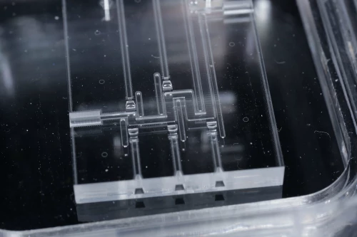
Quantum systems, particularly those based on ion traps and photonic qubits, rely on precise optical addressing. Lasers must target individual ions or photonic modes with sub-micron accuracy. At scale, this means routing light through integrated waveguides, fiber interfaces, and beam splitters embedded in the same substrate that hosts the trap.
The problem: conventional multi-component assemblies introduce mechanical joints. Thermal cycling, vibration, and even the pressure differential at cryogenic temperatures cause these joints to drift. When alignment shifts by even a few micrometers, optical access degrades, gate fidelity drops, and the system requires recalibration or fails entirely.
What quantum engineers need: photonic routing elements that are fabricated monolithically within the trap substrate, with no bonding interfaces that can move.
Differential Thermal Expansion at Cryogenic Temperatures
Ion trap quantum computers operate at temperatures approaching absolute zero. At these temperatures, materials contract. Different materials contract at different rates, governed by their coefficients of thermal expansion (CTE).
Multi-material assemblies electrodes bonded to a ceramic substrate, optical fibers glued into a metal mount accumulate stress across thousands of thermal cycles. Over time, this stress causes delamination, cracking, and dimensional drift that moves electrodes out of their designed positions.
Fused silica has a CTE of approximately 0.55 × 10⁻⁶/°C among the lowest of any engineering material. A monolithic fused silica structure containing both electrodes and optical elements eliminates CTE mismatch entirely. The entire structure moves as one.
Limited Optical Access to the Trap Zone
In a linear ion trap, ions are confined and addressed in a narrow trapping zone defined by the electrode geometry. Getting laser light into and fluorescence out of that zone requires optical access through the trap structure itself. In conventional trap designs, this means engineering gaps or slots in the electrode array that compromise trapping efficiency.
Femtosecond laser microfabrication makes it possible to write optical waveguides directly into the glass substrate, routing light with ±1 µm precision to within micrometers of the ion position. This eliminates the trade-off between trapping efficiency and optical access.
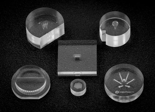
What Is Femtosecond Laser Microfabrication?
Femtosecond laser microfabrication, specifically the Selective Laser Etching (SLE) process, uses ultrashort laser pulses (on the order of 10⁻¹⁵ seconds) to modify the internal structure of transparent glass at a defined focal point. The modified material is then selectively removed by chemical etching, leaving behind three-dimensional structures with sub-micron precision.
Unlike conventional glass machining (grinding, drilling, wet etching), SLE:
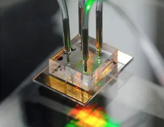
The result is a single-piece glass component that integrates mechanical, electrical, and optical functions — with no assembly, no bonding agents, and no interfaces that can drift or delaminate.
Frequently Asked Questions
What materials are used in femtosecond laser microfabrication for quantum hardware?
Fused silica (synthetic amorphous SiO₂) is the preferred material for quantum hardware applications due to its ultra-low coefficient of thermal expansion (0.55 × 10⁻⁶/°C), optical transparency across UV to near-IR wavelengths, chemical inertness, and vacuum compatibility. FEMTOPRINT also processes borosilicate glass and sapphire for applications requiring different mechanical or optical properties.
How does SLE differ from standard glass etching or MEMS fabrication?
Selective Laser Etching uses femtosecond laser pulses to selectively modify the internal structure of glass at a defined focal point, enabling true 3D feature definition inside the bulk material. Standard wet etching is a surface process and cannot produce enclosed 3D geometries. DRIE (Deep Reactive Ion Etching) is limited to silicon substrates. SLE produces optically smooth internal surfaces, tolerates aspect ratios exceeding 100:1, and can write features at arbitrary depths without surface masking.
Can femtosecond laser microfabrication integrate both optical and electrical functions in the same substrate?
Yes. FEMTOPRINT fabricates monolithic structures that combine 3D optical waveguides (written into the glass bulk), electrode patterns (deposited on glass surfaces or sidewalls), and precision mechanical features (fiber grooves, alignment features, vacuum feedthroughs) in a single fused silica part. This integration eliminates assembly steps and removes bonding interfaces that would otherwise drift under thermal cycling.
Talk with our expert and discover more.