Talk to anyone building AI data center infrastructure in 2026, and they'll tell you the same story. Copper's dead. Signal degrades past 200 Gb/s per lane, heat becomes unbearable, and you can't span beyond a single rack. Optical interconnects are the only way forward. Nvidia's betting billions on CPO. Broadcom's pushing it harder. Corning and Marvell are structuring entire roadmaps around moving optics closer to silicon.
Everyone's focused on the same thing: getting the laser and receiver next to the compute chip instead of stranding them in a pluggable transceiver 30 cm away.
But if you actually build one of these systems, you hit a wall that none of the press releases mention. The bottleneck isn't the optics. It's the mechanical interface that holds them together.
Here's what most people miss: integrating optics and silicon doesn't mean the problem is solved. It means the real work is about to start.
In a traditional CPO architecture—say, Nvidia's Spectrum-X switch with co-packaged lasers—you're still connecting a fiber to a photonic chip. That connection has to be perfect. Submicron perfect. Not just once. Thousands of times per wafer, across dozens of wafers, month after month.
The fiber ferrule and the chip input have different thermal coefficients. The bonding adhesive shrinks unevenly. By the time you're done, you've got:
±0.5 microns was the spec. You're now seeing ±1.2 microns in production. Coupling efficiency drops. You need expensive post-assembly tuning. Or you scrap the part.
The mechanical gap between where the fiber ends and where the waveguide begins is hundreds of microns. Every gap is a loss point. You're trying to couple light across air. Dust on the fiber end face + high-power laser (>300 mW in some designs) = thermal damage. Heat buildup. Burned interfaces. Reliability goes sideways.
In highly integrated architectures, a defect at the fiber interface doesn't just kill one device. It ripples through the whole assembly. Fiber Array Unit (FAU) yield issues compound. If your bonding step has 95% yield, and your alignment step has 92% yield, your combined yield is 87%. Now stack that across six process steps. You're looking at 50-60% final yield on the most critical subsystem.
This is why every investor presentation talks about 'advanced packaging' and 'FAU yields' as the technical bottlenecks. It's not a side problem. It's the primary one.
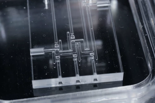
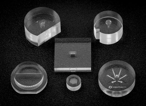
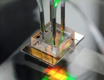
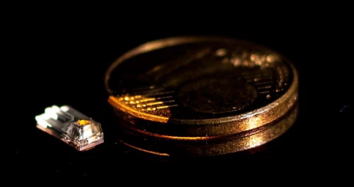
FemtoPrint's approach starts from a different place entirely. Instead of assembling fiber, adhesive, alignment layers, and silicon together, the entire fiber-coupling interface is fabricated directly inside a single piece of glass.
One monolithic component. Three optical functions:
Precision-drilled holes in fused silica, ±0.5 micron repeatability. The fiber sits flush. There's no assembly tolerance stack. No drift over thermal cycles.
Direct laser-written routing paths inside the glass, with true 3D freedom. No bonding interfaces between layers. No adhesive shrinkage. Propagation loss of 0.3 dB/cm—better than most discrete waveguide approaches.
Mirrors and lenses etched directly into the same piece of glass, with surface finish down to 5 nm Ra. Mode-matching, beam shaping, and fiber-to-chip coupling all happen within the same refractive-index profile. No air gaps. No dust.
Everything is integrated into a single part. Manufactured, tested, and shipped as one unit.
The numbers matter here:
This is what solves the bottleneck. Not faster optics. Not denser chip packing. Mechanical integration that actually holds tolerance through manufacturing and field deployment.
The fiber-to-chip problem is about to get worse before it gets better.
AI data centers are consuming fiber capacity faster than the supply chain can scale. Demand for data-center-grade fiber grew 76% year-on-year in 2025. Fiber preform production—the glass rods that become fiber—takes 18 to 24 months to expand. Lead times are already stretching to a full year. The infrastructure is under stress.
At the same time, the next generation of systems needs tighter coupling, higher-channel density, and better reliability. Every micron of alignment loss translates to power consumption, heat dissipation, and operational cost at hyperscale. You can't afford yield loss. You can't afford field failures. You can't afford rework.
Pluggable optics solved the interconnect bottleneck. Co-packaged optics moved the needle on distance and power. But neither solved the mechanical integration problem. That's where the real yield loss is happening.
Monolithic glass isn't an incremental improvement. It's a category shift. It says: stop treating the fiber-to-chip interface as an assembly problem and start treating it as a fabrication problem.
This is still early. Most of the industry is still oriented around modular, plug-and-play approaches. Standardization around CPO form factors is happening. Nvidia, Broadcom, and a handful of other players are setting the roadmap.
But standardization assumes the mechanical problem is solved. It isn't.
For teams actually building CPO systems or exploring alternatives to the standard architecture, the question isn't whether monolithic integration matters. It's whether you can afford not to solve it. Yield in production, tolerance hold-up, and field reliability are no longer negotiable. Not at the scale of AI infrastructure.
The bottleneck has shifted. It's no longer about getting optics closer to silicon. It's about integrating them in a way that actually holds precision in manufacturing and deployment.
Glass monoliths do that today.
FemtoPrint's platform fabricates integrated glass components combining precision ferrule alignment, 3D waveguide routing, and micro-optics in a single monolithic part. ±1 µm relative tolerance, 0.3 dB/cm propagation loss and five integrated optical functions.