If you run hardware for a trapped-ion program, you probably know that number, and it is rarely small. The qubit roadmap promises more ions every year. The optical table does not scale with it. Every new individually addressed ion means more beams through the same viewports, more alignment work, and one more thing that drifts the next time the chamber is baked.
This article covers why optical delivery has become the real scaling bottleneck for trapped-ion systems, what changes when the waveguides move into the trap, and why the substrate material decides whether that approach can carry both UV and IR light.
The hard part of scaling a trapped-ion quantum computer is often not the ions. It is the light. Getting six or more laser beams into the same ~200 µm trapping zone, and keeping them there without drift, is where many programs stall.
A single ¹⁷¹Yb⁺ qubit already needs several wavelengths: 369 nm for Doppler cooling and state detection, 935 nm for repumping, 399 nm for photoionization during loading, and 355 nm or 435 nm for coherent gate operations. Each beam must reach the ion with micrometre pointing stability. Multiply that by every individually addressed ion and the optical system grows faster than the qubit count.
The research community says this plainly. Sandia National Laboratories called optical delivery to many individual ions a major technical challenge for trapped-ion scaling in its 2024 Nature Communications paper. ETH Zurich described the control optics as a barrier to scaling.
For a CTO, the problem shows up in three places:
Free-space laser delivery works for a handful of ions. Beyond that, three problems compound.
The result is an optical setup that grows with every qubit and drifts with every thermal cycle: the opposite of what a scalable architecture needs.
The approach gaining traction is to build the waveguides into the trap. Fibers bring each wavelength to the chip edge, and on-chip waveguides carry it to an out-coupler beneath the ion. This is the same principle behind femtosecond-laser-written glass waveguides in photonics, applied to quantum hardware. Cooling, gate and readout beams then stay fixed relative to the ion because they share its substrate.
In ten years the idea has moved from a single-ion demonstration to multi-ion operation:
Two patterns stand out. Most platforms stack thin-film waveguides (SiN, Al₂O₃) in layers, each covering only part of the spectrum. And the femtosecond-laser route, which writes 3D waveguides inside glass, is now being validated in working ion traps.
Moving the optics into the trap moves the material problem there too. A substrate that carries both electrodes and waveguides must meet four conditions at once:
The fourth condition removes most candidates. Many polymers and lower-grade glasses absorb or solarize in the near-UV, and silicon is opaque below about 1.1 µm. That is the short answer to why fused silica keeps coming up in ion-trap design reviews.
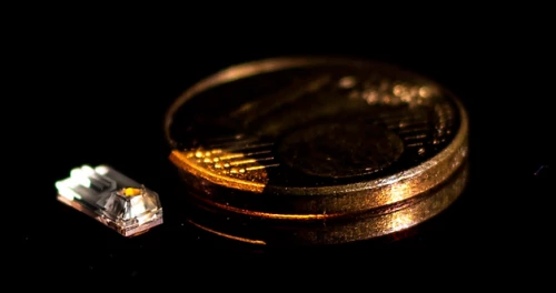
FEMTOPRINT manufactures glass ion traps for quantum computing in fused silica for exactly this reason. Our selective laser etching (SLE) technology and femtosecond laser writing place waveguides, through-glass vias (TGVs) and channels in one monolithic block. There is no bonded interface left to outgas or to drift under thermal cycling.
That difference matters. A bonded hybrid, such as a laser-written glass layer fixed onto an electrode chip, adds an interface whose position and outgassing must be controlled through every bake-out. A monolithic part removes that variable.
What the process delivers today:
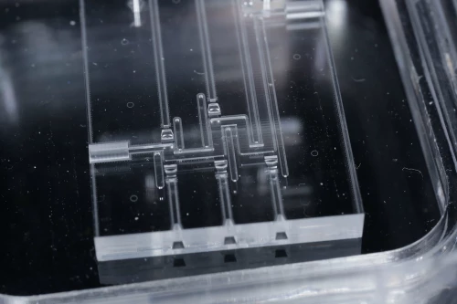
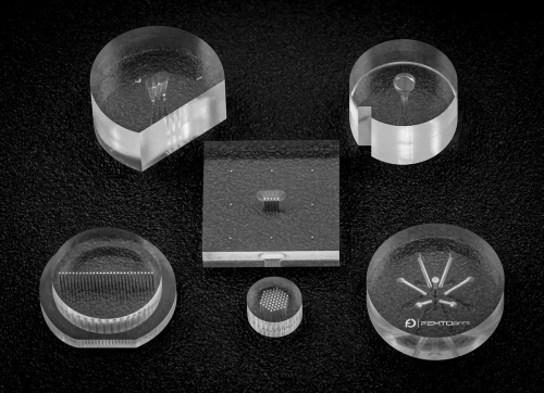
In one fabrication step, a trap can combine 3D waveguides, glass micro-optics such as micro-lenses, V-grooves and fiber hole arrays for passive fiber alignment, and alignment marks on the surface or in the bulk. Fibers can be held in glass fiber ferrules made from the same material, photonic chips can be coupled through a glass interposer, and electrode and mirror layers come from our metallization and optical coating process.
The same platform produces 3D ion traps with overhanging structures, Penning ion traps and ion traps for quantum sensing and atomic clocks. The full list of integrated optical features is on our photonic connectivity for ion traps page.
What wavelength range are you trying to cover in a single substrate? UV addressing and IR cooling together change which materials are even viable.
Send us your ion species, wavelengths and trap geometry and our quantum team will reply with a substrate feasibility check. For the wider picture, see our glass microfabrication for quantum technologies.
Optical delivery. Each ion needs several laser wavelengths for cooling, gates and readout, focused with micrometre stability. Free-space optics through vacuum viewports grow with qubit count and drift after each UHV bake-out.
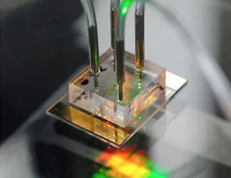
Waveguides built into the trap chip carry laser light from fibers at the chip edge to out-couplers beneath each ion. The beams are fixed relative to the trap electrodes, so they need no realignment from outside the vacuum chamber.
Typically 369 nm for Doppler cooling and detection, 935 nm for repumping, 399 nm for photoionization, and 355 nm or 435 nm for gate operations. A single substrate that carries all of them must transmit from the near-UV to the near-IR.
Fused silica transmits from the UV to the near-IR, is non-magnetic, withstands UHV bake-out above 200 °C and outgasses very little. Its thermal expansion of about 0.55 ppm/K keeps waveguides aligned to electrodes through thermal cycles.
Yes. Femtosecond laser writing creates 3D waveguides inside the bulk of the glass. Research groups have used laser-written waveguides to drive coherent operations on trapped ions, and FEMTOPRINT produces monolithic fused-silica traps with integrated waveguides.
A monolithic trap has no bonded interface. That removes a source of outgassing and of positional drift during bake-out, and keeps optical and electrical features aligned within ±1 µm.
FEMTOPRINT SA, a Swiss glass microfabrication company based in Agno, produces monolithic fused-silica ion traps with integrated waveguides, micro-lenses, fiber-alignment features and electrodes, from prototype to wafer-scale production.
More answers on materials, lead times and trap formats are in our quantum FAQ.