For most groups the honest answer is weeks. You pull the trap, image it, re-measure the electrode gaps and argue about whether a wafer shifted by a micron during bonding. The experiment waits.
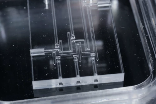
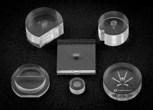
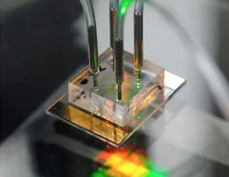
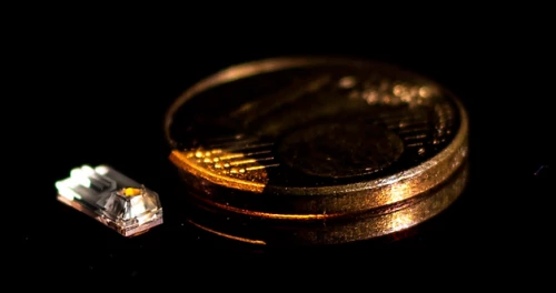
A team at ETH Zürich and the Paul Scherrer Institute (PSI) built a segmented linear Paul trap that shortens that argument. It's a monolithic ion trap: one block of fused silica, shaped in three dimensions by selective laser-induced etching (SLE) at FEMTOPRINT, then metallized. No stacked wafers. No bonding. No layer alignment. Two identical copies now run in two independent labs, and when the measurements drifted from the simulation, the authors went looking for the cause and showed it wasn't the glass.
Key takeaway. In the ETH Zürich–PSI monolithic fused silica ion trap, measured motional frequencies matched boundary-element simulations at the percent level. The residual deviations were traced to stray electric fields of order 50 V/m along the trap axis and to one electrically floating electrode, not to the SLE-fabricated geometry.
The paper, posted to arXiv in September 2026, is A monolithic segmented 3D ion trap fabricated from fused silica by selective laser-induced etching. Below is what they built, what the fabrication process allowed, and the measurement section that anyone choosing a trap fabrication route should read twice.
The device is a four-blade segmented linear Paul trap with a 300 µm ion–electrode distance. Each DC blade is cut into nine segments, giving 18 independently controlled DC electrodes between 250 µm and 750 µm wide, with a wider 500 µm segment at the centre to keep the ions away from trench edges.
The two RF electrodes aren't segmented, but they carry "dummy" trenches at the same axial positions as the DC cuts. Those trenches don't isolate anything. They're there to reduce axial micromotion near segment boundaries. Four large electrodes on top compensate stray fields, and a trace on the front face doubles as an antenna for driving magnetic-dipole transitions.
Now the part that gets lost in a short post. Everything below sits in the same piece of glass:
That's a lot of 3D geometry for one part. On a stacked-wafer design, several of those features would sit on different layers that someone has to align.
It also works. The traps held linear chains of up to 33 ⁴⁰Ca⁺ ions. The segments shaped an anharmonic axial well that spaced ten ions almost evenly, and split a six-ion chain into two three-ion crystals. Single ions stayed trapped for hours to days, at background pressures estimated in the low 10⁻¹⁰ mbar range. Both traps are in routine operation and have already been used in follow-on experiments, including a 2026 Physical Review Letters result on the optical Magnus effect with a trapped ion.
If you're scoping a design like this, our 3D ion traps page lists the process figures, and the ion traps overview covers the other trap families we machine in glass.
Segmented 3D traps give you what surface traps can't: deep trapping wells, low radial anharmonicity and good optical access, plus fine control of the axial potential. The cost has always been the build. Most segmented 3D traps are made from separately fabricated layers that have to be aligned and bonded, and every micron of residual misalignment shows up in the field.
The paper spells out the chain. Electrode misalignment produces a residual RF field along the trap axis. That field drives axial micromotion, which in turn causes systematic shifts such as second-order Doppler shifts. Self-aligning geometries and fiducial-based wafer bonding fix most of it, but they add process steps and cost.
We know that route well. FEMTOPRINT has machined fused silica for ETH Zürich's trapped-ion researchers for years, including stacked-wafer designs. A monolithic trap takes a different bet: write the whole geometry into one substrate and remove the alignment step altogether. Fabrication shrinks to three repeatable processes, SLE, metallization and electroplating, and the geometric accuracy of the finished trap is set mainly by the SLE process.
| Surface-electrode trap | Stacked-wafer 3D trap | Monolithic 3D trap (SLE) | |
| Trap depth | Comparatively low | Deep | Deep |
| Optical access | Limited | Good | Good (NA ≈ 0.46 in this trap) |
| Layer alignment and bonding | Not needed | Required | Not needed |
| Axial segmentation | Very fine, lithographic | Yes | Yes (18 DC segments here) |
| Main process steps | Lithography | Pattern, align, bond | SLE, metallize, electroplate |
Our position is simple. If your roadmap calls for 3D confinement with segmented axial control, evaluate the monolithic route first. If you need dense arrays of sub-100 µm zones today, surface traps still own that space. Fused silica's low dielectric loss and UHV track record are covered on our why glass page, and the same platform builds Paul traps with through-glass vias and the electrical connectivity around the trap.
The electrodes are nothing more than a metal film on the glass. What separates one electrode from the next is the shape of the trench between them.
Each trench has an undercut that the depositing metal can't see. Gold lands on the walls it can reach and misses the shadowed pocket, so there's no continuous conductive path across the gap. No mask. The glass masks itself.
For comparison: in 2021 the same ETH research group metallized a stacked-wafer trap with delicate shadow masks that had to be laser-cut in a separate development. Here that whole step is gone.
The tricky part is geometry around corners. A simple inverted L or T profile shadows fine on a flat run, but where a trench turns around an edge of the trap, the deposition angle changes and full shadowing is no longer guaranteed. That's where short circuits come from. Adding a "serif" (a secondary undercut) solves the shadowing, though the standard serif-T leaves a thin overhang that breaks easily. The team used an inverted-serif T: the second undercut points away from the surface instead of toward it. It shadows from every deposition angle and leaves no fragile lip.
FEMTOPRINT's part in this went beyond running the laser. The authors credit us with carrying out the SLE fabrication, sharing process insight, advising on modifications to the trench profile and optimizing the trenches near corners to suppress short circuits. That last point is the one that decides whether 18 electrodes stay 18 electrodes. It's a fabrication decision as much as a physics one, and it's where an engineering partner earns its place.
Metallization went like this:
Evaporation at shallow angles produced porous, columnar gold on some faces and left two small uncoated patches on the inner bottom surface. The team also tested magnetron sputtering, which gives denser, more uniform films and still self-shadows as long as the mean free path of the sputtered atoms is much larger than the trench dimensions. For coating options on glass parts, see our metallization and optical coating page.
The most useful page of the paper for a trap designer is the one listing what the process imposed. These aren't brochure numbers. They come from a group that redesigned the trap several times to live within them.
SLE works in two steps. A tightly focused femtosecond laser modifies the glass along the path you write, then a wet etch removes the modified material much faster than the untouched glass. That speed ratio, the selectivity, decides what you can build.
| Parameter | Value in this trap | What it means for your design |
| Etch selectivity, modified vs. unmodified fused silica | ~10³ | High aspect ratios are possible, but every exposed surface still etches a little |
| Unmodified glass removed in the deep structures | ~15 µm | Sets the floor on how narrow a deep trench can be |
| Minimum trench gap at the surface | ~30 µm | Achieved on most trenches of this trap |
| Laser-affected zone | ~3 µm across, ~40 µm along the beam | Features are anisotropic: orientation matters |
| Minimum feature along the laser axis | ~60 µm | Axial trenches on top of the trap used a 60 µm gap, made deeper and staggered in depth |
| Pre-metallization inspection | X-ray micro-CT | Finds trenches whose entrance didn't open or whose second undercut came out short |
Two lessons stand out.
First, the 30 µm figure is a property of deep self-shadowing trenches, not of SLE in general. The longer the etch, the more untouched glass you lose, so a shallower feature can go narrower. When we review a trap design, trench depth and trench width are discussed together.
Second, orientation is a design variable. With a laser-affected zone of 3 µm by 40 µm, a trench that runs across the beam can be twice as narrow as one that runs along it. Put your tightest gaps where the laser helps you.
There were also problems, and the paper says so. Writing large modified volumes builds mechanical stress, and early versions fractured, so the team thickened the top of the trap at some cost to optical access. Micro-CT on an early test sample showed a few malformed trenches, likely from optical aberrations distorting the laser-affected zone. Both are the kind of issue you want caught in a design-for-manufacturing review rather than after the gold goes on. The authors also point to sapphire, whose selectivity exceeds 10⁴, as a possible route to smaller features, while noting that complex 3D structures like this one haven't been shown in sapphire yet.
No. Measured motional frequencies agreed with simulation at the percent level, and every residual deviation was explained by electrical effects: a stray field below 300 V/m (axial component mostly under 50 V/m) and one floating electrode. Simulated geometry errors at stacked-wafer alignment tolerances shifted frequencies far less than what was measured.
That's the short answer. The way they got there is the part to copy.
Picture the usual situation. Your axial frequency is 3% off the model at one end of the trap. Is the electrode where the CAD says it is? Is the wafer stack tilted? Or is something charging up? Without a way to separate those, you're back to pulling the trap. The ETH Zürich–PSI team separated them with measurements they already had:
Their conclusion is the sentence a CTO should underline: the predictability of the trapping potential is limited by electrical effects, mainly stray fields and the floating electrode, rather than by the accuracy of the SLE-defined geometry.
In schedule terms, that removes a branch from your debugging tree. When a monolithic trap misbehaves, you look at wire bonds, coating coverage and stray charge. You don't re-measure the glass. (The floating electrodes, by the way, were one DC segment in Trap 1 and one compensation electrode in Trap 2, most likely failed wire bonds.)
Reading the paper as a fabricator, these are the decisions we'd put on the table at the first design review:
One more point for anyone thinking past the first prototype. SLE is maskless: the same laser file that makes your first trap makes the hundredth, with no new tooling in between. That's why two identical traps could go into two labs. We run rapid prototyping for first articles and contract manufacturing at wafer scale under ISO 9001 and ISO 13485, on the same platform.
A monolithic ion trap is an ion trap whose 3D electrode structure is machined from a single piece of material, here fused silica, instead of being assembled from aligned and bonded layers. With no internal bond line, there's no inter-layer alignment error and no bonded interface inside the trap.
A femtosecond laser writes the trap geometry inside a fused silica block, and a wet etch removes the laser-modified glass. The structure is then metallized, for example with evaporated or sputtered gold, and electroplated. Self-shadowing trenches isolate the electrodes during coating, so no shadow mask is needed.
It depends on depth and orientation. In the ETH Zürich–PSI trap, deep self-shadowing trenches reached a ~30 µm surface gap across the laser axis and ~60 µm along it. Shallower features can be narrower. We size width and depth together in a feasibility review.
Not in this study. Mode frequencies matched simulation at the percent level, and the authors traced the remaining deviations to stray electric fields and a floating electrode. Simulated geometry errors at stacked-wafer tolerances produced much smaller shifts. More answers are on our quantum FAQ.
Send us your project and we'll tell you what SLE can hold. A CAD or STEP file is ideal, but a sketch with the ion–electrode distance, segment count, trench layout and planned metallization is enough to start. Our engineers will come back with trench profiles, feature limits along the laser axis and a route from first article to volume.
Send your trap design for a feasibility review →
Still weighing whether glass microfabrication fits your hardware? Start with the 5 questions CTOs ask us about precision glass microfabrication, or browse our full quantum applications.
E. Brucke, M. Wagener, M. Fontboté-Schmidt, P. Leindecker, M. Marinelli, V. Negnevitsky, I. Sergachev, G. F. M. Tomassi, P. Venetz, S. Welte, J. Home, D. Kienzler and C. Hempel, "A monolithic segmented 3D ion trap fabricated from fused silica by selective laser-induced etching", arXiv:2609.01694 (2026). ETH Zürich–PSI Quantum Computing Hub and Institute for Quantum Electronics, ETH Zürich.