Every quarter, a handful of CTOs and R&D leads sit down with our engineering team to work out whether femtosecond laser glass microfabrication is the right process for their next optical, photonic, or microfluidic part.
Here are the five questions we heard most often in the first half of 2026, answered the way we'd answer them on a call. If you want the short version first, there's a table further down.
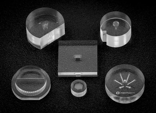
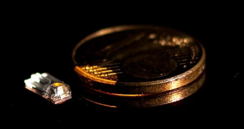
It's a manufacturing process that uses a focused femtosecond laser, combined with Selective Laser Etching (SLE), to write 3D microstructures, channels, waveguides, lenses, mechanical features, directly inside a glass substrate, at micron-level tolerances, without gluing or bonding separate pieces together.
That's the definition. Now the five questions.
Yes. XY tolerance stays at ±1 µm and Z tolerance at ±2 µm from the first unit through unit 10,000, because the femtosecond laser process is subtractive and digitally controlled. There's no tool physically wearing down the way a drill bit or a mill would over a long run.
We get asked this constantly, and for good reason a lot of prototyping technologies look great on part #1 and drift by part #500. Vertical integration is what closes that gap: laser writing, etching, and metrology all happen in one Swiss facility, under the same process parameters, batch after batch. When a CTO wants proof, we don't argue the point, we show the process-control data from the last production run.
Sa <100 nm on the as-etched, patterned surface. After surface treatment, Sa <10 nm.
It's worth being precise here, because plenty of spec sheets quote "Ra" when they mean something closer to "Sa" and the two aren't interchangeable. Ra is a line profile, a single 2D trace across a surface. Sa is an areal average across the whole measured surface, defined under ISO 25178, and it's the number that actually predicts optical performance. Sa <10 nm is fine enough for waveguide facets, micro-mirrors, and ferrule end-faces, where even light scatter from a rough surface shows up as signal loss. If a vendor's datasheet just says "sub-10 nm roughness" without saying which metric, ask which one.
It scales. Working area up to 300 mm in diameter, substrates up to 30 mm thick, wafer-scale batches. Our systems engineers and laser specialists spend most of their time on one problem: cutting cycle time per part without touching tolerance, through multi-head machining and process parallelization, the groundwork for hundreds of thousands of units a year.
Here's the honest part. For a client scaling from 10,000 to 200,000 units a year, the bottleneck usually isn't part quality, it's lead time while capacity comes online. We'd rather say that on the first call than have a program find out three months into a ramp. This is also why the current wave of interest from photonics teams building for AI data-center connectivity, and from quantum hardware groups, is pushing capacity planning harder than it has in years. The CTOs asking this question in 2026 aren't ordering hundreds of parts, they're planning for hundreds of thousands.
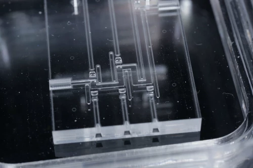
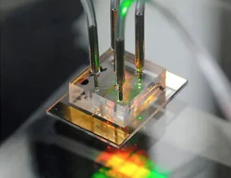
Yes, and it's usually the reason photonics and life-science teams come to us in the first place. Waveguides, lenses, mirrors, microfluidic channels, and mechanical mounting or fiber-alignment features can sit inside one monolithic glass block, with relative positioning between features held under ±1 µm.
No assembly. No bonding interface that can leak or drift under thermal cycling. No stack-up tolerance to budget across three or four separately machined parts. If a current design routes light and fluid through a part built from several bonded pieces, there's a real chance the whole thing collapses into one.
Anything that isn't glass. Metals, ceramics, and polymers sit outside the process, if a design needs a hybrid glass-metal assembly, that's a conversation about interfaces and secondary joining, not something solved in a single glass part. Feature resolution also has a floor around 1 µm; a design that needs true sub-micron geometry isn't a fit for glass microfabrication today.
We'd rather put that on slide one than have a program find out three months in.
|
Question |
Short answer |
|
Can you hold ±1 µm at production volume? |
Yes — XY ±1 µm / Z ±2 µm from unit 1 to unit 10,000. |
|
How fine is the surface finish? |
Sa <100 nm as-etched; Sa <10 nm after surface treatment. |
|
Does it scale past prototyping? |
Yes — wafer-scale, up to 300 mm working area; lead time is the real constraint, not quality. |
|
Can optics and fluidics share one part? |
Yes — monolithic integration, <±1 µm relative positioning, no bonding. |
|
What can't it do? |
Anything that isn't glass; feature resolution floor around 1 µm. |
Femtosecond laser writing modifies the glass at the molecular level along a 3D path inside the material. SLE then selectively etches away the modified regions, leaving the unmodified glass as the final structure. Combined, they're what makes true 3D geometry possible, not the 2.5D shapes you get from surface-only processes.
Fused silica, fused quartz, borosilicate (including Borofloat® 33), aluminosilicate, alkali-free glass, and ULE. Material choice usually comes down to optical transmission range, CTE matching to an adjacent component, or biocompatibility for a diagnostics application.
Yes. ISO 13485:2016 for medical devices and ISO 9001:2015. That matters if a part is heading into a diagnostics or medtech pipeline where design-history-file traceability is part of the audit.
Five is a good start. It's not the full list. Before choosing any glass microfabrication partner, us included, there are another ten questions worth asking about metrology at your specific geometry, yield expectations, metallization and coating compatibility, IP handling, and feasibility-review turnaround. Those are usually the ones that separate a smooth six-month ramp from a painful one.