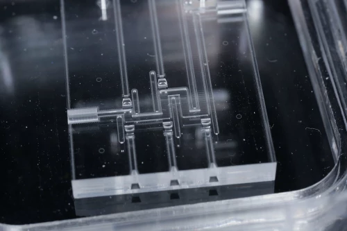
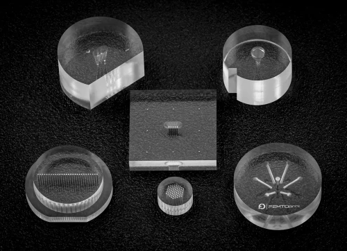
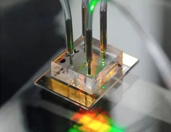
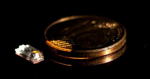
In short: in miniaturized medical devices, the parts that fail are usually the joints: fluidic ports, fiber-to-chip couplings, bonded lids, adhesive seals. 3D glass microfabrication removes many of those joints by building microchannels, optical waveguides and micro-optics inside a single fused silica substrate. Their alignment is then fixed at fabrication, within ±1 µm in XY, instead of being set by hand at assembly.
When a point-of-care cartridge or an optofluidic biosensor fails verification, the detector and the pump are rarely to blame. The trouble sits between them. A fiber drifts a few microns after thermal cycling. Adhesive wicks into a channel. A bonded lid starts to delaminate at the edge of a sensing chamber.
Each of these is an interface problem, and each one gets harder as devices shrink. Better assembly can push the problem back a step. Removing the interface makes it go away.
Because every interface adds its own tolerance, and the tolerances add up. Take a typical optofluidic detection path: a fiber sits in a groove, the groove is aligned to a chip, the chip is bonded to a lid, and the detection window has to line up with a channel in another layer. Each step contributes an error. The tolerance stack-up of four steps is what decides whether the excitation light hits the sample or the channel wall.
In multi-material micro-assemblies (polymer, metal and glass parts joined together), four failure modes come up again and again:
The table below summarizes how the two architectures compare. It is not one-sided: for some devices, assembly is still the better choice (see the section on limits).
|
|
Multi-material micro-assembly |
Monolithic 3D glass microdevice |
|
Optical-to-fluidic alignment set by |
Assembly step, per unit |
Laser toolpath, at fabrication |
|
Bonded or glued interfaces in the optical path |
Several |
None for internal features |
|
Thermal expansion mismatch |
Between every material pair |
Single material |
|
Autofluorescence background |
Depends on polymer and adhesive |
Low (fused silica) |
|
Cost of a design change |
New mold or mask set |
New toolpath file |
|
Unit cost at very high volume |
Lowest (injection molding) |
Higher; scales with laser-written volume |
Fused silica transmits from the deep UV to the near infrared, has very low autofluorescence and is chemically inert to most reagents and cleaning agents. Its coefficient of thermal expansion is about 0.5 ppm/K, so optical and fluidic features hold their geometry across operating temperatures.
That combination matters most in glass microfluidic chips for point-of-care diagnostics and in biophotonics, where fluorescence, absorbance or Raman readouts depend on a clean optical path through the sample.
One caveat. Fused silica is a well-documented biocompatible material, but biocompatibility is qualified for the finished device, under ISO 10993, by its manufacturer. The material gives you a good starting point. It does not replace the testing.
Fused silica is not the only option. FEMTOPRINT also processes borosilicate (Borofloat® 33), aluminosilicate, alkali-free glass and ULE, which can be a better fit when cost, bonding partner or expansion match drive the choice. More on material selection: why glass.
It builds the optical and fluidic features in the same piece of glass, in the same machine run, from the same coordinate system. FEMTOPRINT does this with femtosecond laser micromachining combined with selective laser etching (SLE):
There is no photomask and no lithography. A design change is a new toolpath file, which is why the same process serves rapid prototyping and production. The approach is well documented in the literature: researchers have used femtosecond-written waveguides and etched channels in one fused silica chip to trap and stretch single cells (Bellini et al., Biomedical Optics Express, 2012).
When a second part is unavoidable, for example to encapsulate electronics, a femtosecond laser weld can join glass to glass or glass to silicon at room temperature without adhesive. See hermetic sealing.
|
Parameter |
Value |
|
Tolerance |
XY ±1 µm, Z ±2 µm |
|
Minimum feature size |
<5 µm |
|
Surface roughness |
Sa <100 nm as etched, Sa <10 nm after post-treatment |
|
Aspect ratio |
≥1:500 |
|
Waveguide propagation loss |
<0.2 dB/cm |
|
Working area |
Up to 300 mm wafers, substrates up to 30 mm thick |
|
Quality system |
ISO 13485:2016, ISO 9001:2015 |
When the device is a high-volume disposable with a unit-cost target of cents and no tight optical alignment. Injection-molded polymer wins there, and we would tell you so. Laser writing time scales with the volume of glass you modify, so a large, simple chip with wide channels gains little from it.
The practical middle ground is often a hybrid: put the alignment-critical optofluidic core in glass and keep reservoirs, housing and connectors in polymer. That keeps the expensive tolerance where it pays for itself.
The same platform runs from first prototypes to wafer-scale contract manufacturing, so the geometry you validate is the geometry you buy in volume. FEMTOPRINT’s quality system is certified to ISO 13485:2016, and medical parts are made for product lifecycles of 10 years and more.
To be precise about responsibilities: regulatory approval of the device (CE marking under MDR or IVDR, FDA clearance) stays with you as the manufacturer. A supplier working under ISO 13485 makes design transfer, traceability and change control much easier to document. For the full MedTech offer, see glass microfabrication for medical devices.
We will walk through real design cases, from fluidic layout to optical path, and show where moving to a monolithic glass part removes assembly steps, and the trade-offs that come with it.
It is built for engineers working on point-of-care diagnostic chips, optofluidic biosensors and miniature or implantable medical devices. Bring a current design problem: the Q&A is the most useful part.
Register on the IVAM event page →
Already have a design? Send it to our engineers for a feasibility review →
A process that creates three-dimensional microstructures inside glass, such as buried channels, cavities, holes and optical waveguides. At FEMTOPRINT it combines femtosecond laser writing with selective laser etching, without masks or lithography, and holds XY tolerances of ±1 µm.
A microdevice that combines microfluidic channels with optical elements (waveguides, lenses, windows) on one substrate, so light can excite or read a sample as it flows. Optofluidic chips are used for fluorescence, absorbance and Raman detection in diagnostics and cell analysis.
Fused silica has very low autofluorescence, transmits from UV to near infrared, is chemically inert and expands about 0.5 ppm/K. Polymers are cheaper at very high volume but add optical background and expand far more with temperature.
FEMTOPRINT’s process holds XY ±1 µm and Z ±2 µm, with minimum features below 5 µm, aspect ratios of 1:500 and above, and surface roughness down to Sa <10 nm after post-treatment.
Yes. FEMTOPRINT is certified to ISO 13485:2016 and ISO 9001:2015 and runs prototyping and wafer-scale production on the same platform. Regulatory approval of the finished device remains with the device manufacturer.
Not always. For cartridges with cent-level cost targets and no tight optical alignment, injection-molded polymer is usually cheaper. A hybrid design, with the alignment-critical optofluidic core in glass and the rest in polymer, is often the better trade-off.